ZHCSLD2E may 2020 – july 2023 UCC28782
PRODUCTION DATA
- 1
- 1 特性
- 2 应用
- 3 描述
- 4 Revision History
- 5 Device Comparison Table
- 6 Pin Configuration and Functions
- 7 Specifications
-
8 Detailed Description
- 8.1 Overview
- 8.2 Functional Block Diagram
- 8.3
Detailed Pin Description
- 8.3.1 BUR Pin (Programmable Burst Mode)
- 8.3.2 FB Pin (Feedback Pin)
- 8.3.3 REF Pin (Internal 5-V Bias)
- 8.3.4 VDD Pin (Device Bias Supply)
- 8.3.5 P13 and SWS Pins
- 8.3.6 S13 Pin
- 8.3.7 IPC Pin (Intelligent Power Control Pin)
- 8.3.8 RUN Pin (Driver and Bias Source for Isolator)
- 8.3.9 PWMH and AGND Pins
- 8.3.10 PWML and PGND Pins
- 8.3.11 SET Pin
- 8.3.12 RTZ Pin (Sets Delay for Transition Time to Zero)
- 8.3.13 RDM Pin (Sets Synthesized Demagnetization Time for ZVS Tuning)
- 8.3.14 BIN, BSW, and BGND Pins
- 8.3.15 XCD Pin
- 8.3.16 CS, VS, and FLT Pins
- 8.4
Device Functional Modes
- 8.4.1 Adaptive ZVS Control with Auto-Tuning
- 8.4.2 Dead-Time Optimization
- 8.4.3 EMI Dither and Dither Fading Function
- 8.4.4 Control Law across Entire Load Range
- 8.4.5 Adaptive Amplitude Modulation (AAM)
- 8.4.6 Adaptive Burst Mode (ABM)
- 8.4.7 Low Power Mode (LPM)
- 8.4.8 First Standby Power Mode (SBP1)
- 8.4.9 Second Standby Power Mode (SBP2)
- 8.4.10 Startup Sequence
- 8.4.11 Survival Mode of VDD (INT_STOP)
- 8.4.12 Capacitor Voltage Balancing Function
- 8.4.13 Device Functional Modes for Bias Regulator Control
- 8.4.14
System Fault Protections
- 8.4.14.1 Brown-In and Brown-Out
- 8.4.14.2 Output Over-Voltage Protection (OVP)
- 8.4.14.3 Input Over Voltage Protection (IOVP)
- 8.4.14.4 Over-Temperature Protection (OTP) on FLT Pin
- 8.4.14.5 Over-Temperature Protection (OTP) on CS Pin
- 8.4.14.6 Programmable Over-Power Protection (OPP)
- 8.4.14.7 Peak Power Limit (PPL)
- 8.4.14.8 Output Short-Circuit Protection (SCP)
- 8.4.14.9 Over-Current Protection (OCP)
- 8.4.14.10 External Shutdown
- 8.4.14.11 Internal Thermal Shutdown
- 8.4.15 Pin Open/Short Protections
-
9 Application and Implementation
- 9.1 Application Information
- 9.2
Typical Application Circuit
- 9.2.1 Design Requirements for a 65-W USB-PD Adapter Application
- 9.2.2
Detailed Design Procedure
- 9.2.2.1 Input Bulk Capacitance and Minimum Bulk Voltage
- 9.2.2.2 Transformer Calculations
- 9.2.2.3 Clamp Capacitor Calculation
- 9.2.2.4 Bleed-Resistor Calculation
- 9.2.2.5 Output Filter Calculation
- 9.2.2.6 Calculation of ZVS Sensing Network
- 9.2.2.7 Calculation of BUR Pin Resistances
- 9.2.2.8 Calculation of Compensation Network
- 9.2.3 Application Curves
- 10Power Supply Recommendations
- 11Layout
- 12Device and Documentation Support
- 13Mechanical, Packaging, and Orderable Information
8.4.2 Dead-Time Optimization
The dead-time optimizer in Figure 8-18 controls the two dead-times: the dead-time between PWMH falling edge and PWML rising edge (tZ), as well as the dead-time between PWML falling edge and PWMH rising edge (tD(PWML-H)).
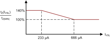
Similar to UCC28780, the adaptive control law for tZ of UCC28782 utilizes the line feed-forward signal to extend tZ as VBULK reduces, as shown in Figure 8-20. The VS pin senses VBULK through the auxiliary winding voltage (VAUX) when the low-side switch (QL) is on. The auxiliary winding creates a line-sensing current (IVSL) out of the VS pin flowing through the upper resistor of the voltage divider on VS pin (RVS1). Minimum tZ (tZ(MIN)) is set at VBULK(MAX) through the RTZ pin. When IVSL is lower than 666 μA, tZ linearly increases and the maximum tZ extension is 140% of tZ(MIN).
 Figure 8-20 tZ Control Optimized for Wide Input Voltage Range
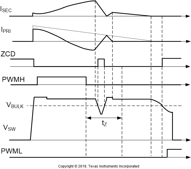
 Figure 8-21 The Enhanced tZ Control for CCM Avoidance
The enhanced tZ control of UCC28782 helps to avoid voltage stress on the secondary rectifier due to temporary continuous conduction mode (CCM) operation. If the high side switch turns off under a higher than normal negative resonant current instance, the switch node voltage (VSW) and the auxiliary winding voltage (VAUX) will drop very fast, because a higher di/dt current flows through the leakage inductance. At the same instant, if the magnetizing current has not decayed down to zero yet, the current will continue to flow in the secondary rectifier, so the switch node voltage will recover back to a high level again and results in a short-duration voltage dip behavior within the tZ period. If a ACF controller turns on the low-side switch after tZ expires but the magnetizing current is still positive, the limited turn off speed of the synchronous rectifier (SR) will result in a higher di/dt current as the low-side switch turns on, so a high voltage spike is generated on the SR drain-to-source voltage. Then, the FET voltage rating or the snubber design on the secondary side may need to be compromised, which are the typical concerns of flyback topology in CCM. Therefore, the VS pin of UCC28782 can detect this event and avoid low-side switch turn on after tZ expires under this situation.
The concept is to detect the ZCD signal once again at the instant of tZ expiration, such that the controller will not respond to the false ZCD signal after the high side switch turns off. When the duration of the voltage dip is shorter than tZ setting, the ZCD signal will change back to its original low state at the tZ expiration instance. When there is no valid switch node voltage transition detected from the ZCD signal at the instance, the controller will wait for another ZCD rising edge to trigger the low-side switch turn-on of the next cycle. Since the next ZCD signal could be a real indication of the magnetizing current reached to 0 A, the CCM turn-off event of secondary rectifier will not occur. Figure 8-21 illustrates the issue and the operation principle of the improved switching control in UCC28782.
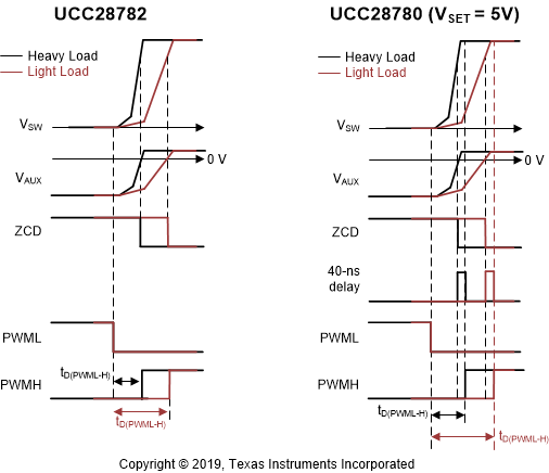
The control law for tD(PWML-H) of UCC28782 is adaptive with the slope variation of the switching node voltage, regardless of the SET-pin voltage. One reason of applying the adaptive control is to generate a minimum dead time for reducing the body diode conduction time of the high-side Si switch or the reverse conduction time of the high-side GaN switch. Another reason is to avoid the risk of hard switching. Since the rising slope of the switch node voltage varies with different peak magnetizing currents as output load changes, using a fixed dead-time can potentially cause hard-switching on the high-side clamp switch (QH) if the dead-time is not long enough.
 Figure 8-22 tD(PWML-H) Control Optimized for GaN and Si FETs
For the GaN ACF with UCC28780, a fixed 40-ns dead time from PWML falling edge to PWMH rising edge is applied for the SET pin connected to GND. For the Si ACF with UCC28780, the adaptive dead time adjustment based on the ZCD falling edge plus 40-ns delay is applied for the SET pin connected to the REF pin. The enhanced tD(PWML-H) control of UCC28782 helps to further reduce the body diode conduction time of the high side Si switch or the reverse conduction time of the high-side GaN switch without risk of hard switching on the high side switch. Moreover, the same dead time control is generalized for both SET-pin connections. After the ZCD falling edge is detected, the PWMH driver of UCC28782 will pull high immediately, and the extra 40-ns delay in UCC28780 is removed. For the GaN ACF with UCC28782, as long as the VS-pin delay from the parasitic capacitive loading is reduced by a proper layout arrangement, it is possible to shorten the reverse conduction time in heavy load, and also eliminate the concern of high-side hard switching in light load. For the Si ACF with UCC28782, the propagation delay of the high-side driver already provides enough margin for switch node voltage settled to a high level after ZCD falling edge is triggered, so there is no need to introduce an extra 40-ns delay like UCC28780.