ZHCSLG6B June 2020 – April 2022 UCC27288
PRODUCTION DATA
- 1 特性
- 2 应用
- 3 说明
- 4 Revision History
- 5 Pin Configuration and Functions
- 6 Specifications
- 7 Detailed Description
- 8 Application and Implementation
- 9 Power Supply Recommendations
- 10Layout
- 11Device and Documentation Support
- 12Mechanical, Packaging, and Orderable Information
8.2.2.5 Delays and Pulse Width
The total delay encountered in the PWM, driver and power stage need to be considered for a number of reasons, primarily delay in current limit response. Also to be considered are differences in delays between the drivers which can lead to various concerns depending on the topology. The synchronous buck topology switching requires careful selection of dead-time between the high-side and low-side switches to avoid cross conduction as well as excessive body diode conduction.
Bridge topologies can be affected by a volt-second imbalance on the transformer if there is imbalance in the high-side and low-side pulse widths in any operating condition. The UCC27288 device has maximum propagation delay, across process, and temperature variation, of 30 ns and delay matching of 7 ns, which is one of the best in the industry.
Narrow input pulse width performance is an important consideration in gate driver devices, because output may not follow input signals satisfactorily when input pulse widths are very narrow. Although there may be relatively wide steady state PWM output signals from controller, very narrow pulses may be encountered under following operating conditions.
- soft-start period
- large load transients
- short circuit conditions
These narrow pulses appear as an input signal to the gate driver device and the gate driver device need to respond properly to these narrow signals.
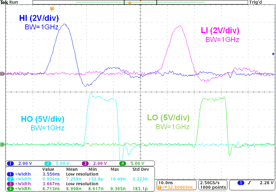
Figure 8-2 shows that the UCC27288 device produces reliable output pulse even when the input pulses are very narrow. The propagation delay and delay matching do not get affected when the input pulse width is very narrow.
 Figure 8-2 Input and Output Pulse Width