ZHCSLL2A May 2021 – March 2022 TPS25830A-Q1 , TPS25832A-Q1
PRODUCTION DATA
- 1 特性
- 2 应用
- 3 说明
- 4 Revision History
- 5 说明(续)
- 6 Device Comparison Table
- 7 Pin Configuration and Functions
- 8 Specifications
- 9 Parameter Measurement Information
-
10Detailed Description
- 10.1 Overview
- 10.2 Functional Block Diagram
- 10.3
Feature Description
- 10.3.1 Buck Regulator
- 10.3.2 Enable/UVLO and Start-Up
- 10.3.3 Switching Frequency and Synchronization (RT/SYNC)
- 10.3.4 Spread-Spectrum Operation
- 10.3.5 VCC, VCC_UVLO
- 10.3.6 Minimum ON-Time, Minimum OFF-Time
- 10.3.7 Internal Compensation
- 10.3.8 Bootstrap Voltage (BOOT)
- 10.3.9 RSNS, RSET, RILIMIT and RIMON
- 10.3.10 Overcurrent and Short Circuit Protection
- 10.3.11 Overvoltage, IEC and Short to Battery Protection
- 10.3.12 Cable Compensation
- 10.3.13 USB Port Control
- 10.3.14 FAULT Response
- 10.3.15 USB Specification Overview
- 10.3.16 USB Type-C® Basics
- 10.3.17 Device Power Pins (IN, CSN/OUT, and PGND)
- 10.3.18 Thermal Shutdown
- 10.3.19 Power Wake
- 10.4 Device Functional Modes
-
11Application and Implementation
- 11.1 Application Information
- 11.2
Typical Application
- 11.2.1 Design Requirements
- 11.2.2
Detailed Design Procedure
- 11.2.2.1 Output Voltage
- 11.2.2.2 Switching Frequency
- 11.2.2.3 Inductor Selection
- 11.2.2.4 Output Capacitor Selection
- 11.2.2.5 Input Capacitor Selection
- 11.2.2.6 Bootstrap Capacitor Selection
- 11.2.2.7 VCC Capacitor Selection
- 11.2.2.8 Enable and Undervoltage Lockout Set-Point
- 11.2.2.9 Current Limit Set-Point
- 11.2.2.10 Cable Compensation Set-Point
- 11.2.2.11 LD_DET, POL, and FAULT Resistor Selection
- 11.2.3 Application Curves
- 12Power Supply Recommendations
- 13Layout
- 14Device and Documentation Support
- 15Mechanical, Packaging, and Orderable Information
10.3.11.1 VBUS and VCSN/OUT Overvoltage Protection
The TPS2583xA-Q1 integrates overvoltage protection on both BUS and CSN/OUT pin to meet different application requirement.
BUS pin can withstand up to 18 V, and the OVP threshold is 7-V typical. Once overvoltage is detected on BUS pin, the LS_GD will turn off immediately, also FAULT asserts after 8-ms deglitch time. Once the excessive voltage is removed, the LS_GD will turn on again and FAULT deasserts.
CSN/OUT pin can withstand up to 20 V, and the OVP threshold is 7.5-V typical. Once overvoltage is detected on CSN/OUT pin, the buck converter will stop regulation, also LS_GD will turn off immediately. Once the excessive voltage is removed, the buck converter will resume and LS_GD turn on again.
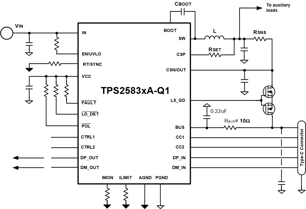
 Figure 10-22 Current Limit with External MOSFET
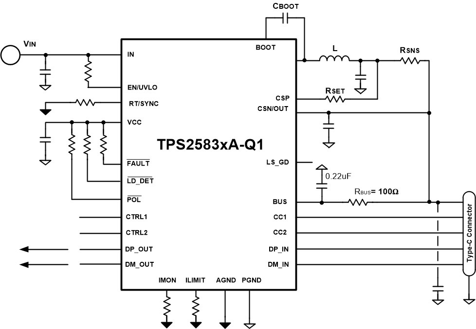
 Figure 10-23 Buck Average Current Limit
TPS2583xA-Q1 is configured in external FET current limit mode as shown in #T5423571-114. When short to battery occurs on BUS_Connector, the external MOSFET will be turn off immediately after BUS pin detect overvoltage. The FAULT signal will assert after 8ms deglitch time, see Figure 11-35. With Back-to-back FET, the TPS2583xA-Q1 can withstand short to battery event even when Vin is off. A 10-Ω 0805 resistor is recommended between BUS pin and BUS_Connector.
TPS2583xA-Q1 is configured in buck average current limit mode as shown in #T5423571-115. When short to battery occurs on BUS_Connector, the buck regulator will stop switching after CSN/OUT pin detect overvoltage. The FAULT signal will also assert after 8-ms deglitch time. A 100-Ω 0805 resistor is recommended between BUS pin and BUS_Connector in buck average current limit mode.