ZHCSLP5D June   2007  – June 2021 TRS3232E

PRODUCTION DATA  

  1. 特性
  2. 应用
  3. 说明
  4. Revision History
  5. Pin Configuration and Functions
  6. Specifications
    1. 6.1 Absolute Maximum Ratings
    2. 6.2 ESD Ratings
    3. 6.3 ESD Ratings - IEC Specifications
    4. 6.4 Recommended Operating Conditions
    5. 6.5 Thermal Information
    6. 6.6 Electrical Characteristics — Device
    7. 6.7 Electrical Characteristics — Driver
    8. 6.8 Electrical Characteristics — Receiver
    9. 6.9 Switching Characteristics
  7. Parameter Measurement Information
  8. Detailed Description
    1. 8.1 Overview
    2. 8.2 Functional Block Diagram
    3. 8.3 Feature Description
      1. 8.3.1 Power
      2. 8.3.2 RS232 Driver
      3. 8.3.3 RS232 Receiver
    4. 8.4 Device Functional Modes
      1. 8.4.1 VCC Powered by 3 V to 5.5 V
      2. 8.4.2 VCC Unpowered, VCC = 0 V
  9. Application and Implementation
    1. 9.1 Application Information
    2. 9.2 Typical Application
      1. 9.2.1 Design Requirements
      2. 9.2.2 Detailed Design Procedure
      3. 9.2.3 Application Curve
  10. 10Power Supply Recommendations
  11. 11Layout
    1. 11.1 Layout Guidelines
    2. 11.2 Layout Example
  12. 12Device and Documentation Support
    1. 12.1 接收文档更新通知
    2. 12.2 支持资源
    3. 12.3 Trademarks
    4. 12.4 Electrostatic Discharge Caution
    5. 12.5 Glossary
  13. 13Mechanical, Packaging, and Orderable Information

Device Functional Modes

Table 8-1 and Table 8-2 list the functional modes of the drivers and receivers of TRS3232E.

Table 8-1 Each Driver(1)
INPUT
DIN
OUTPUT
DOUT
LH
HL
H = high level, L = low level
Table 8-2 Each Receiver(1)
INPUT
RIN
OUTPUT
ROUT
LH
HL
OpenH
H = high level, L = low level,
Open = input disconnected or connected driver off
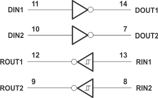
GUID-511A1191-4DA9-471A-A7E0-60840663F1F0-low.gifFigure 8-1 Logic Diagram