ZHCSLY5A August 2020 – July 2021 TPS65994AD
PRODUCTION DATA
- 1 特性
- 2 应用
- 3 说明
- 4 Revision History
- 5 Pin Configuration and Functions
-
6 Specifications
- 6.1 Absolute Maximum Ratings
- 6.2 ESD Ratings
- 6.3 Recommended Operating Conditions
- 6.4 Recommended Capacitance
- 6.5 Thermal Information
- 6.6 Power Supply Characteristics
- 6.7 Power Consumption
- 6.8 PP_5V Power Switch Characteristics
- 6.9 PP_EXT Power Switch Characteristics
- 6.10 Power Path Supervisory
- 6.11 CC Cable Detection Parameters
- 6.12 CC VCONN Parameters
- 6.13 CC PHY Parameters
- 6.14 Thermal Shutdown Characteristics
- 6.15 ADC Characteristics
- 6.16 Input/Output (I/O) Characteristics
- 6.17 I2C Requirements and Characteristics
- 6.18 Typical Characteristics
- 7 Parameter Measurement Information
-
8 Detailed Description
- 8.1 Overview
- 8.2 Functional Block Diagram
- 8.3
Feature Description
- 8.3.1 USB-PD Physical Layer
- 8.3.2 Power Management
- 8.3.3
Power Paths
- 8.3.3.1
Internal Sourcing Power Paths
- 8.3.3.1.1 PP_5Vx Current Clamping
- 8.3.3.1.2 PP_5Vx Local Overtemperature Shut Down (OTSD)
- 8.3.3.1.3 PP_5Vx Current Sense
- 8.3.3.1.4 PP_5Vx OVP
- 8.3.3.1.5 PP_5Vx UVLO
- 8.3.3.1.6 PP_5Vx Reverse Current Protection
- 8.3.3.1.7 Fast Role Swap
- 8.3.3.1.8 PP_CABLE Current Clamp
- 8.3.3.1.9 PP_CABLE Local Overtemperature Shut Down (OTSD)
- 8.3.3.1.10 PP_CABLE UVLO
- 8.3.3.2 Sink Path Control
- 8.3.3.1
Internal Sourcing Power Paths
- 8.3.4 Cable Plug and Orientation Detection
- 8.3.5 Default Behavior Configuration (ADCIN1, ADCIN2)
- 8.3.6 ADC
- 8.3.7 DisplayPort Hot-Plug Detect (HPD)
- 8.3.8 Digital Interfaces
- 8.3.9 Digital Core
- 8.3.10 I2C Interface
- 8.4 Device Functional Modes
- 9 Application and Implementation
- 10Power Supply Recommendations
- 11Layout
- 12Device and Documentation Support
- 13Mechanical, Packaging, and Orderable Information
8.4.2 Power States
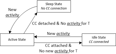
The TPS65994AD may operate in one of three different power states: Active, Idle, or Sleep. The Modern Standby mode is a special case of the Idle mode. The functionality available in each state is summarized in the following table. The device will automatically transition between the three power states based on the circuits that are active and required, see the following figure. In the Sleep State the TPS65994AD will detect a Type-C connection. Transitioning between the Active mode to the Idle mode requires a period of time (T) without any of the following activity:
- Incoming USB PD message.
- Change in CC status.
- GPIO input event.
- I2C transactions.
- Voltage alert.
- Fault alert.
 Figure 8-28 Flow
Diagram For Power States
Figure 8-28 Flow
Diagram For Power States| Active Source Mode(1) | Active Sink Mode(6) | Idle Source Mode(2) | Idle Sink Mode(7) | Modern Standby Source Mode(4) | Modern Standby Sink Mode(5) | Sleep Mode(3) | |
|---|---|---|---|---|---|---|---|
| PP_5V1 | enabled | disabled | enabled | disabled | enabled | disabled | disabled |
| PP_5V2 | enabled | disabled | enabled | disabled | disabled | disabled | disabled |
| PP_EXT1 | disabled | enabled | disabled | enabled | disabled | disabled | disabled |
| PP_EXT2 | disabled | enabled | disabled | enabled | disabled | disabled | disabled |
| PP_CABLE1 | enabled | enabled | enabled | enabled | disabled | disabled | disabled |
| PP_CABLE2 | enabled | enabled | enabled | enabled | disabled | disabled | disabled |
| external PA_CC1 termination | Rd | Rp 3.0A | Rd | Rp 3.0A | Rd | Rp 3.0A | open |
| external PA_CC2 termination | open | open | open | open | open | open | open |
| external PB_CC1 termination | Rd | Rp 3.0A | Rd | Rp 3.0A | open | open | open |
| external PB_CC2 termination | open | open | open | open | open | open | open |