ZHCSLY9A October 2020 – December 2020 LM7310
PRODUCTION DATA
- 1 特性
- 2 应用
- 3 说明
- 4 Revision History
- 5 Pin Configuration and Functions
- 6 Specifications
-
7 Detailed Description
- 7.1 Overview
- 7.2 Functional Block Diagram
- 7.3
Feature Description
- 7.3.1 Input Reverse Polarity Protection
- 7.3.2 Undervoltage Protection (UVLO & UVP)
- 7.3.3 Overvoltage Lockout (OVLO)
- 7.3.4 Inrush Current control and Fast-trip
- 7.3.5 Analog Load Current Monitor Output
- 7.3.6 Reverse Current Protection
- 7.3.7 Overtemperature Protection (OTP)
- 7.3.8 Fault Response
- 7.3.9 Power Good Indication (PG)
- 7.4 Device Functional Modes
- 8 Application and Implementation
- 9 Power Supply Recommendations
- 10Layout
- 11Device and Documentation Support
- 12Mechanical, Packaging, and Orderable Information
5 Pin Configuration and Functions
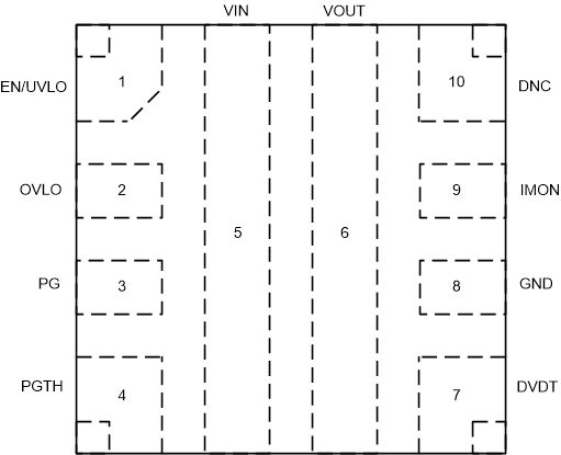
 Figure 5-1 LM73100 RPW Package 10-Pin QFN Top
View
Figure 5-1 LM73100 RPW Package 10-Pin QFN Top
ViewTable 5-1 Pin Functions
| PIN | TYPE | DESCRIPTION | |
|---|---|---|---|
| NAME | NO. | ||
| EN/UVLO |
1 | Analog Input | Active High Enable for the device. A Resistor Divider on this pin from input supply to GND can be used to adjust the Undervoltage Lockout threshold. Do not leave floating. Refer to Section 7.3.2 for more details. |
|
OVLO |
2 | Analog Input | A Resistor Divider on this pin from supply to GND can be used to adjust the Overvoltage Lockout threshold. This pin can also be used as an Active Low Enable for the device. Do not leave floating. Refer to Section 7.3.3 for more details. |
|
PG |
3 | Digital Output | Power Good indication. This is an Open Drain signal which is asserted High when the internal powerpath is fully turned ON and PGTH input exceeds a certain threshold. Refer to Section 7.3.9 for more details. |
|
PGTH |
4 | Analog Input | Power Good Threshold. Refer to Section 7.3.9 for more details. |
|
IN |
5 |
Power | Power Input. |
|
OUT |
6 |
Power | Power Output. |
|
DVDT |
7 | Analog Output | A capacitor from this pin to GND sets the output turn on slew rate. Leave this pin floating for the fastest turn on slew rate. Refer to Section 7.3.4.1 for more details. |
|
GND |
8 |
Ground | This is the ground reference for all internal circuits and must be connected to system GND. |
|
IMON |
9 | Analog Output |
Analog load current monitor. The pin voltage can be used to monitor the output load current. An external resistor from this pin to ground sets the current monitor gain. Recommended to connect external clamp to limit the voltage below abs max rating in case of large current spikes. Connect to ground if not used. Do not leave floating. Refer to Section 7.3.5 for more details. |
|
DNC |
10 |
X |
Internal test pin. Do not connect anything on this pin. |