ZHCSLY9A October 2020 – December 2020 LM7310
PRODUCTION DATA
- 1 特性
- 2 应用
- 3 说明
- 4 Revision History
- 5 Pin Configuration and Functions
- 6 Specifications
-
7 Detailed Description
- 7.1 Overview
- 7.2 Functional Block Diagram
- 7.3
Feature Description
- 7.3.1 Input Reverse Polarity Protection
- 7.3.2 Undervoltage Protection (UVLO & UVP)
- 7.3.3 Overvoltage Lockout (OVLO)
- 7.3.4 Inrush Current control and Fast-trip
- 7.3.5 Analog Load Current Monitor Output
- 7.3.6 Reverse Current Protection
- 7.3.7 Overtemperature Protection (OTP)
- 7.3.8 Fault Response
- 7.3.9 Power Good Indication (PG)
- 7.4 Device Functional Modes
- 8 Application and Implementation
- 9 Power Supply Recommendations
- 10Layout
- 11Device and Documentation Support
- 12Mechanical, Packaging, and Orderable Information
8.3 Active ORing
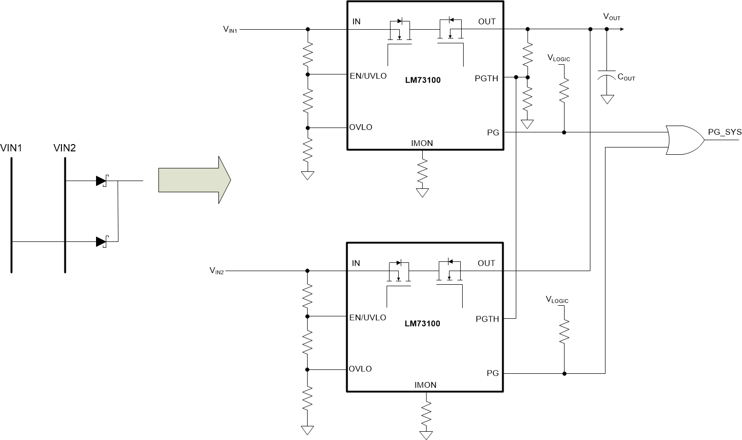
A typical redundant power supply configuration is shown in Figure 8-7 below. Schottky ORing diodes have been popular for connecting parallel power supplies, such as parallel operation of wall adapter with a battery or a hold-up storage capacitor. Similar ORing requirements can be seen in end equipements such as PC, Notebook, Docking stations, Monitors etc.. which can take power from multiple USB ports and/or power adapter. The disadvantage of using ORing diodes is high voltage drop and associated power loss. The LM73100 with integrated, low-ohmic, back-to-back FETs provides a simple and efficient solution. Figure below shows the Active ORing implementation using the devices.
 Figure 8-7 Two Devices, Active ORing
Configuration
Figure 8-7 Two Devices, Active ORing
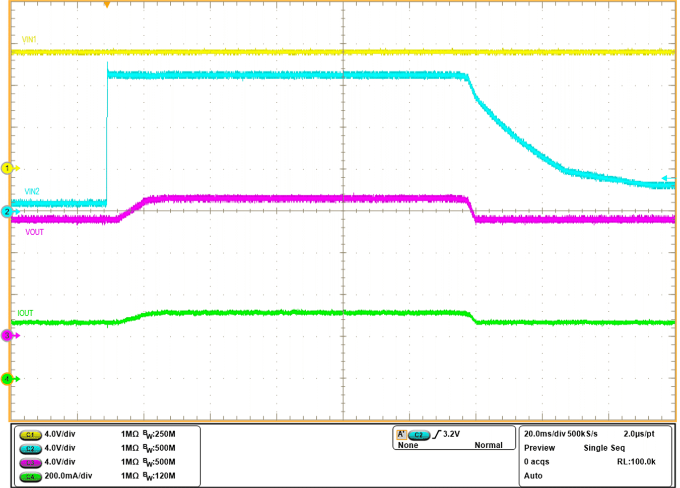
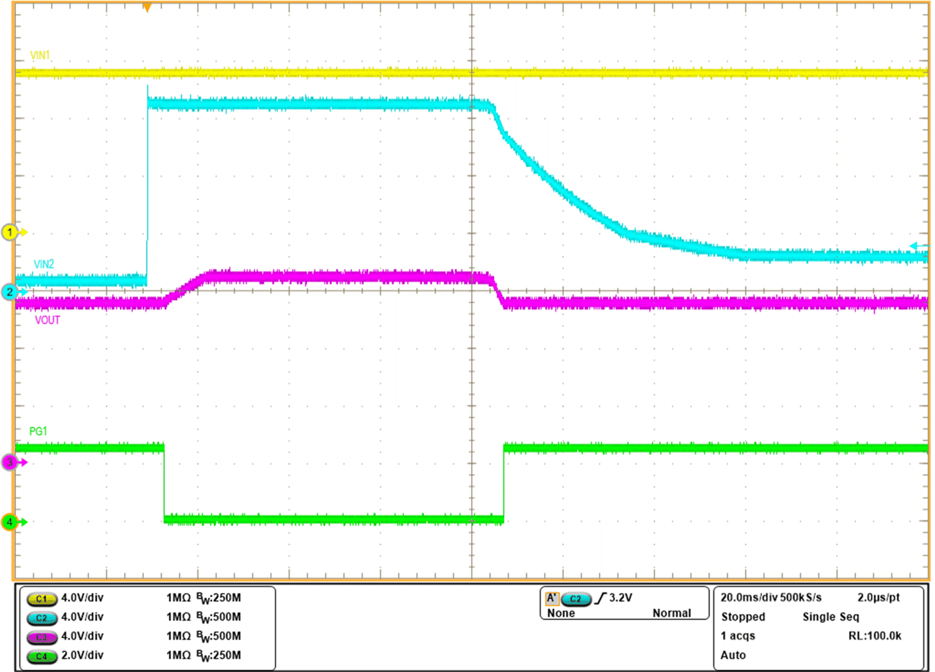
ConfigurationThe linear ORing mechanism in LM73100 ensures that there's no reverse current flowing from one power source to the other during fast or slow ramp of either supply.
The following waveforms illustrate the active ORing behavior.

| VIN1 = 12 V, ROUT = 25 Ω, COUT = 440 μF, IN2 stepped up to 13 V and then ramped down |

| VIN1 = 12 V, ROUT = 25 Ω, COUT = 440 μF, IN2 stepped up to 13 V and then ramped down |
When bus voltages (IN1 and IN2) are matched, device in each rail sees a forward voltage drop and is ON delivering the load current. During this period, current is shared between the rails in the ratio of differential voltage drop across each device.
In addition to supply ORing, the devices protect the system from overvoltage, excessive inrush current and transient overcurrent events during steady state.
- ORing can be done either between two similar rails (such as 12 V & 12 V; 3.3 V & 3.3 V) or between dissimilar rails (such as 12 V & 5 V).
- For ORing cases with skewed voltage combinations, care must be taken to design circuit components on PGTH, EN/UVLO & OVLO pins for the lower voltage channel device such that the absolute maximum ratings on those pins are not exceeded when higher voltage is present on the other channel. Also, the dVdt pin capacitor rating should be chosen based on the highest of the 2 supplies. Refer to Absolute Maximum Ratings and Recommended Operating Conditions tables for more details.