ZHCSLZ8A September 2020 – August 2021 TPS65988DK
PRODUCTION DATA
- 1 特性
- 2 应用
- 3 说明
- 4 Revision History
- 5 Pin Configuration and Functions
-
6 Specifications
- 6.1 Absolute Maximum Ratings
- 6.2 ESD Ratings
- 6.3 Recommended Operating Conditions
- 6.4 Thermal Information
- 6.5 Power Supply Requirements and Characteristics
- 6.6 Power Consumption Characteristics
- 6.7 Power Switch Characteristics
- 6.8 Cable Detection Characteristics
- 6.9 USB-PD Baseband Signal Requirements and Characteristics
- 6.10 Thermal Shutdown Characteristics
- 6.11 Oscillator Characteristics
- 6.12 I/O Characteristics
- 6.13 I2C Requirements and Characteristics
- 6.14 SPI Controller Timing Requirements
- 6.15 HPD Timing Requirements
- 6.16 Typical Characteristics
- 7 Parameter Measurement Information
-
8 Detailed Description
- 8.1 Overview
- 8.2 Functional Block Diagram
- 8.3
Feature Description
- 8.3.1 USB-PD Physical Layer
- 8.3.2 Power Management
- 8.3.3 Port Power Switches
- 8.3.4 Cable Plug and Orientation Detection
- 8.3.5 Dead Battery Operation
- 8.3.6 ADC
- 8.3.7 DisplayPort HPD
- 8.3.8 Digital Interfaces
- 8.3.9 Digital Core
- 8.3.10 I2C Interfaces
- 8.3.11 SPI Controller Interface
- 8.3.12 Thermal Shutdown
- 8.3.13 Oscillators
- 8.4 Device Functional Modes
- 9 Application and Implementation
- 10Power Supply Recommendations
-
11Layout
- 11.1 Layout Guidelines
- 11.2 Layout Example
- 11.3 Stack-up and Design Rules
- 11.4 Main Component Placement
- 11.5 Super Speed Type-C Connectors
- 11.6 Capacitor Placement
- 11.7 CC1/2 Capacitors & ADCIN1/2 Resistors
- 11.8 CC and SBU Protection Placement
- 11.9 CC Routing
- 11.10 DRAIN1 and DRAIN2 Pad Pours
- 11.11 VBUS Routing
- 11.12 Completed Layout
- 11.13 Power Dissipation
- 12Device and Documentation Support
- 13Mechanical, Packaging, and Orderable Information
8.3.10.5 I2C Pin Address Setting (ADCIN2)
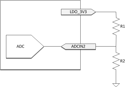
To enable the setting of multiple I2C addresses using a single TPS65988DK pin, a resistor divider is placed externally on the ADCIN2 pin. The internal ADC then decodes the address from this divider value. Figure 8-28 shows the decoding.
 Figure 8-28 I2C Address Divider
Table 8-6 lists the external divider needed to set bits [3:1] of the I2C Unique Address.
Table 8-6 I2C Address Selection
| DIV = R2/(R1+R2)(1) | I2C1 UNIQUE ADDRESS (7bit) | I2C2 UNIQUE ADDRESS (7bit) | |||
|---|---|---|---|---|---|
| DIV_min | DIV_max | I2C1 PORT 1 | I2C1 PORT 2 | I2C2 PORT 1 | I2C2 PORT 2 |
| Short to GND | 0.18 | 0x20 | 0x24 | 0x38 | 0x3F |
| 0.20 | 0.38 | 0x21 | 0x25 | 0x3F | 0x38 |
| 0.40 | 0.58 | 0x22 | 0x26 | 0x4F | 0x48 |
| 0.6 | Short to LDO_3V3 | 0x23 | 0x27 | 0x48 | 0x4F |
(1) External resistor
tolerance of 1% is required. Resistor values must be chosen to yield a DIV
value centered nominally between listed MIN and MAX values.