ZHCSLZ8A September 2020 – August 2021 TPS65988DK
PRODUCTION DATA
- 1 特性
- 2 应用
- 3 说明
- 4 Revision History
- 5 Pin Configuration and Functions
-
6 Specifications
- 6.1 Absolute Maximum Ratings
- 6.2 ESD Ratings
- 6.3 Recommended Operating Conditions
- 6.4 Thermal Information
- 6.5 Power Supply Requirements and Characteristics
- 6.6 Power Consumption Characteristics
- 6.7 Power Switch Characteristics
- 6.8 Cable Detection Characteristics
- 6.9 USB-PD Baseband Signal Requirements and Characteristics
- 6.10 Thermal Shutdown Characteristics
- 6.11 Oscillator Characteristics
- 6.12 I/O Characteristics
- 6.13 I2C Requirements and Characteristics
- 6.14 SPI Controller Timing Requirements
- 6.15 HPD Timing Requirements
- 6.16 Typical Characteristics
- 7 Parameter Measurement Information
-
8 Detailed Description
- 8.1 Overview
- 8.2 Functional Block Diagram
- 8.3
Feature Description
- 8.3.1 USB-PD Physical Layer
- 8.3.2 Power Management
- 8.3.3 Port Power Switches
- 8.3.4 Cable Plug and Orientation Detection
- 8.3.5 Dead Battery Operation
- 8.3.6 ADC
- 8.3.7 DisplayPort HPD
- 8.3.8 Digital Interfaces
- 8.3.9 Digital Core
- 8.3.10 I2C Interfaces
- 8.3.11 SPI Controller Interface
- 8.3.12 Thermal Shutdown
- 8.3.13 Oscillators
- 8.4 Device Functional Modes
- 9 Application and Implementation
- 10Power Supply Recommendations
-
11Layout
- 11.1 Layout Guidelines
- 11.2 Layout Example
- 11.3 Stack-up and Design Rules
- 11.4 Main Component Placement
- 11.5 Super Speed Type-C Connectors
- 11.6 Capacitor Placement
- 11.7 CC1/2 Capacitors & ADCIN1/2 Resistors
- 11.8 CC and SBU Protection Placement
- 11.9 CC Routing
- 11.10 DRAIN1 and DRAIN2 Pad Pours
- 11.11 VBUS Routing
- 11.12 Completed Layout
- 11.13 Power Dissipation
- 12Device and Documentation Support
- 13Mechanical, Packaging, and Orderable Information
11.10 DRAIN1 and DRAIN2 Pad Pours
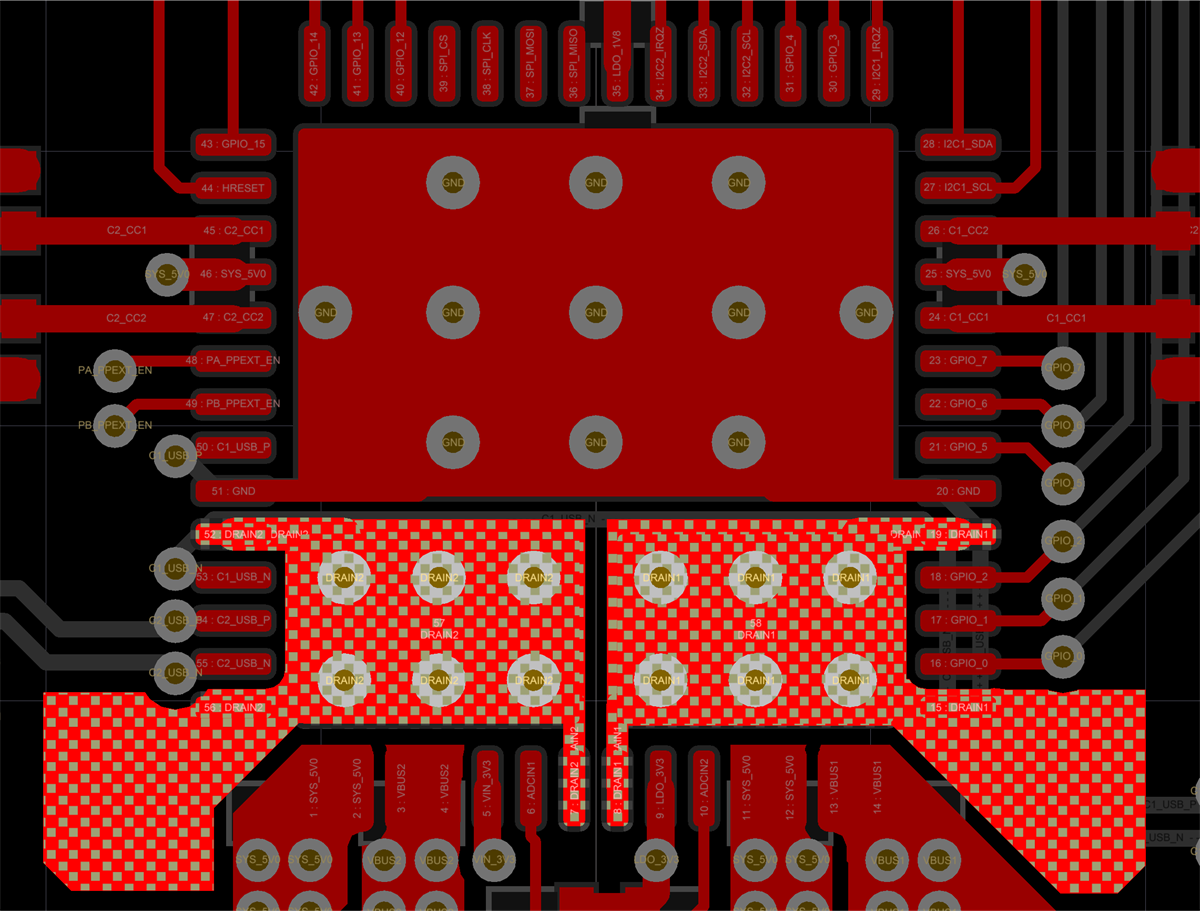
The drain pads are used for dissipating heat from the two power paths. DRAIN1 and DRAIN2 should NEVER be connected to each other or to GND. They should be left floating with their own nets assigned. The top layer should have all of the DRAIN1 pins tied to the DRAIN1 pan and the DRAIN2 pins tied to the DRAIN2 pad. When high currents are expected in the system it is recommended to place “fins” on the DRAIN1 and DRAIN2 pads. The effective heat dissipation distance is roughly 3 mm from the pad so it does not have to extend to a large area. Figure 11-15 shows the top layer routing for DRAIN1 and DRAIN2.
 Figure 11-15 DRAIN1 and DRAIN2 Top Layer
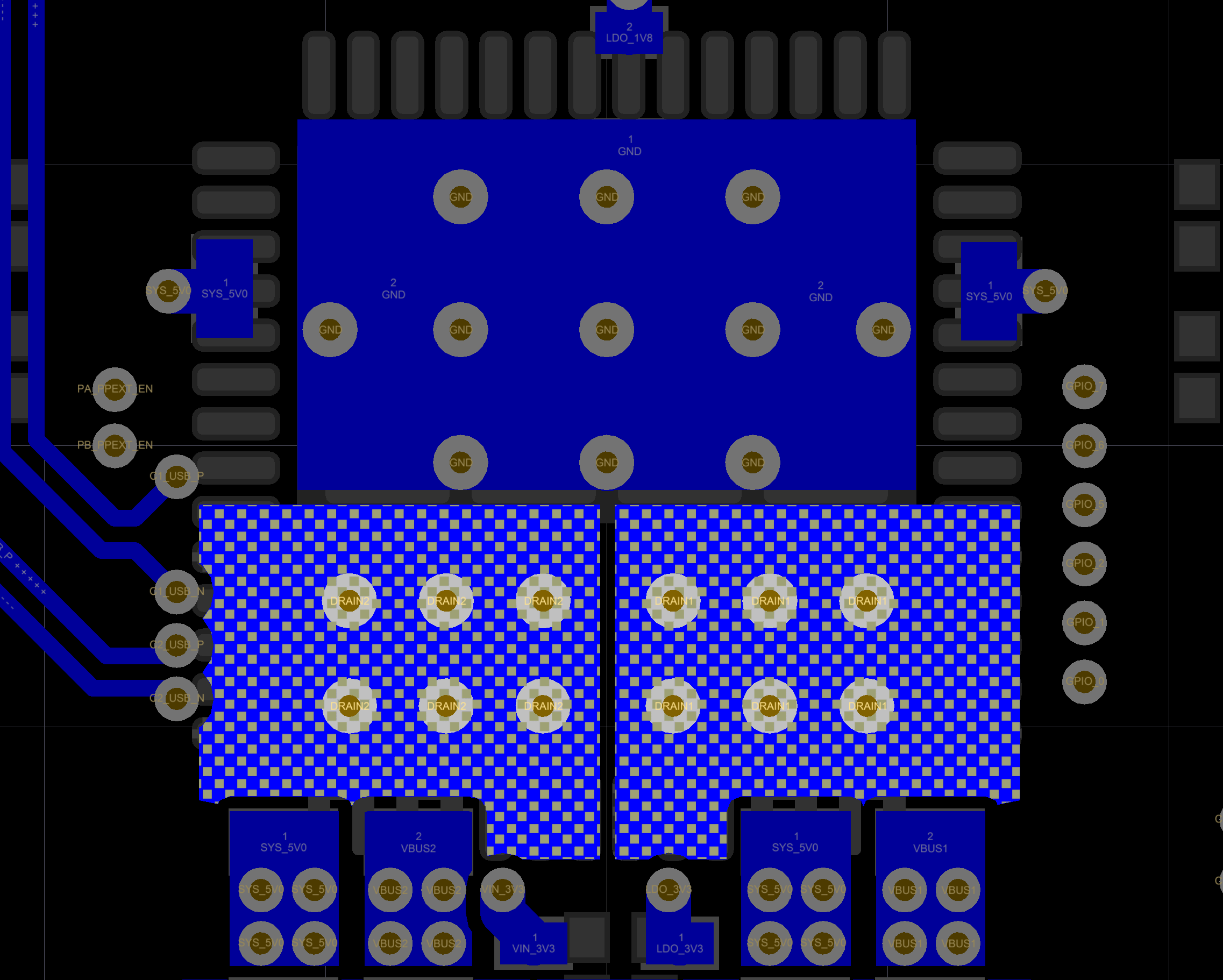
On the bottom layer DRAIN1 and DRAIN2 pour are also required and it is recommended to have a larger pour than the DRAIN1 and DRAIN2 pads. The bottom layer will provide most of the heat dissipation and space should be reserved for the pours. Figure 11-16 shows the bottom layer routing for the DRAIN1 and DRAIN2 pads.
 Figure 11-16 Figure 13. DRAIN1 and DRAIN2 Bottom Layer