ZHCSM06C december   2020  – may 2023 TPS272C45

PRODUCTION DATA  

  1.   1
  2. 特性
  3. 应用
  4. 说明
  5. Revision History
  6. Device Comparison Table
  7. Pin Configuration and Functions
    1. 6.1 Recommended Connections for Unused Pins
  8. Specifications
    1. 7.1 Absolute Maximum Ratings
    2. 7.2 ESD Ratings
    3. 7.3 Recommended Operating Conditions
    4. 7.4 Thermal Information
    5. 7.5 Electrical Characteristics
    6. 7.6 SNS Timing Characteristics
    7. 7.7 Switching Characteristics
    8. 7.8 Typical Characteristics
  9. Parameter Measurement Information
  10. Detailed Description
    1. 9.1 Overview
    2. 9.2 Functional Block Diagram
    3. 9.3 Feature Description
      1. 9.3.1 Programmable Current Limit
        1. 9.3.1.1 Inrush Current Handling
        2. 9.3.1.2 Calculating RILIMx
        3. 9.3.1.3 Configuring ILIMx From an MCU
      2. 9.3.2 Low Power Dissipation
      3. 9.3.3 Protection Mechanisms
        1. 9.3.3.1 Short-Circuit Protection
          1. 9.3.3.1.1 VS During Short-to-Ground
        2. 9.3.3.2 Inductive Load Demagnetization
        3. 9.3.3.3 Thermal Shutdown
        4. 9.3.3.4 Undervoltage Lockout on VS (UVLO)
        5. 9.3.3.5 Undervoltage Lockout on Low Voltage Supply (VDD_UVLO)
        6. 9.3.3.6 Power-Up and Power-Down Behavior
        7. 9.3.3.7 Overvoltage Protection (OVPR)
      4. 9.3.4 Diagnostic Mechanisms
        1. 9.3.4.1 Current Sense
          1. 9.3.4.1.1 RSNS Value
            1. 9.3.4.1.1.1 Current Sense Output Filter
        2. 9.3.4.2 Fault Indication
          1. 9.3.4.2.1 Fault Event Diagrams
        3. 9.3.4.3 Short-to-Supply or Open-Load Detection
          1. 9.3.4.3.1 Detection With Switch Enabled
          2. 9.3.4.3.2 Detection With Switch Disabled
        4. 9.3.4.4 Current Sense Resistor Sharing
    4. 9.4 Device Functional Modes
      1. 9.4.1 Off
      2. 9.4.2 Diagnostic
      3. 9.4.3 Active
      4. 9.4.4 Fault
  11. 10Application and Implementation
    1. 10.1 Application Information
      1. 10.1.1 IEC 61000-4-5 Surge
      2. 10.1.2 Inverse Current
      3. 10.1.3 Loss of GND
      4. 10.1.4 Paralleling Channels
      5. 10.1.5 Thermal Information
    2. 10.2 Typical Application
      1. 10.2.1 Design Requirements
      2. 10.2.2 Detailed Design Procedure
        1. 10.2.2.1 RILIM Calculation
        2. 10.2.2.2 Diagnostics
          1. 10.2.2.2.1 Selecting the RISNS Value
      3. 10.2.3 Application Curves
    3. 10.3 Power Supply Recommendations
    4. 10.4 Layout
      1. 10.4.1 Layout Guidelines
      2. 10.4.2 Layout Example
  12. 11Device and Documentation Support
    1. 11.1 Documentation Support
      1. 11.1.1 Related Documentation
    2. 11.2 接收文档更新通知
    3. 11.3 支持资源
    4. 11.4 Trademarks
    5. 11.5 静电放电警告
    6. 11.6 术语表
  13. 12Mechanical, Packaging, and Orderable Information

Inductive Load Demagnetization

When switching off an inductive load, the inductor can impose a negative voltage on the output of the switch. The TPS272C45 includes voltage clamps between VS and VOUT to limit the voltage across the FETs and demagnetize load inductance if there is any. The negative voltage applied at the OUT pin drives the discharge of inductor current. Figure 9-10 shows the device discharging a 40-mH load.
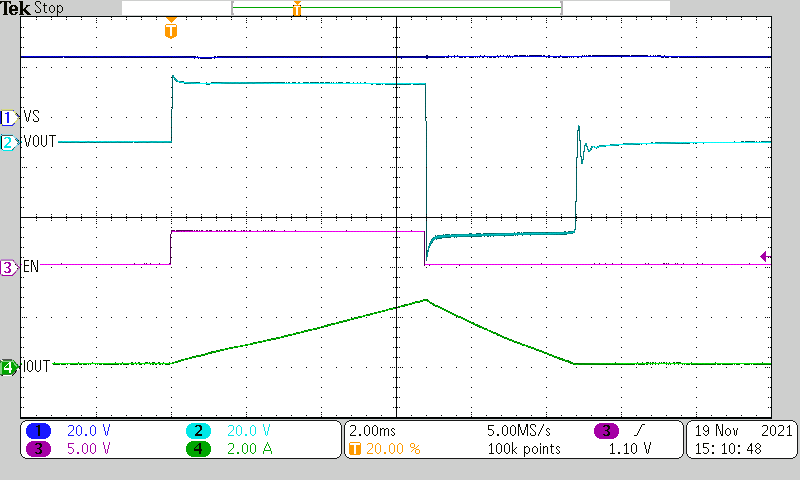
GUID-20211121-SS0I-V3BN-ZTBH-NK40FTMZ2WXS-low.pngFigure 9-10 TPS272C45 Inductive Discharge (40 mH)
The maximum acceptable load inductance is a function of the energy dissipated in the device and therefore the load current and the inductive load. The maximum energy and the load inductance the device can withstand for one pulse inductive dissipation at 125°C is shown in Figure 9-11.The device can withstand 50% of this energy for one million inductive repetitive pulses with a >4-Hz repetitive pulse. If the application parameters exceed this device limit, use a protection device like a freewheeling diode to dissipate the energy stored in the inductor.
GUID-20211203-SS0I-GJBH-Z2F3-2LKFBN58KQJG-low.svgFigure 9-11 TPS272C45 Inductive Load Discharge Energy Capability at 125°C

For more information on driving inductive loads, refer to TI's How to Drive Inductive, Capacitive, and Lighting Loads With Smart High-Side Switches application report.