ZHCSM11A October 2020 – May 2024 TMUX1575
PRODUCTION DATA
8.3.1 Layout Guidelines
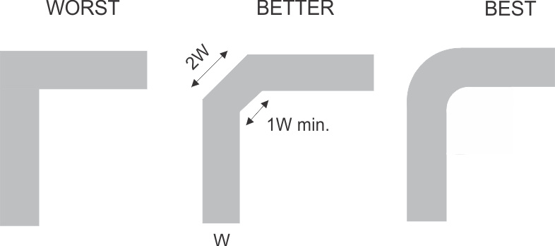
When a PCB trace turns a corner at a 90° angle, a reflection can occur. A reflection occurs primarily because of the change of width of the trace. At the apex of the turn, the trace width increases to 1.414 times the width. This increase upsets the transmission-line characteristics, especially the distributed capacitance and self–inductance of the trace which results in the reflection. Not all PCB traces can be straight and therefore some traces must turn corners. Figure 8-2 shows progressively better techniques of rounding corners. Only the last example (BEST) maintains constant trace width and minimizes reflections.
 Figure 8-2 Trace Example
Route the high-speed signals using a minimum of vias and corners which reduces signal reflections and impedance changes. When a via must be used, increase the clearance size around it to minimize its capacitance. Each via introduces discontinuities in the signal’s transmission line and increases the chance of picking up interference from the other layers of the board. Be careful when designing test points, through-hole pins are not recommended at high frequencies.
Do not route high speed signal traces under or near crystals, oscillators, clock signal generators, switching regulators, mounting holes, magnetic devices or ICs that use or duplicate clock signals.
Avoid stubs on the high-speed signals traces because they cause signal reflections.
Route all high-speed signal traces over continuous GND planes, with no interruptions.
Avoid crossing over anti-etch, commonly found with plane splits.
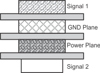
When working with high frequencies, a printed circuit board with at least four layers is recommended; two signal layers separated by a ground and power layer as shown in Figure 8-3.
 Figure 8-3 Example
Layout
Figure 8-3 Example
LayoutThe majority of signal traces must run on a single layer, preferably Signal 1. Immediately next to this layer must be the GND plane, which is solid with no cuts. Avoid running signal traces across a split in the ground or power plane. When running across split planes is unavoidable, sufficient decoupling must be used. Minimizing the number of signal vias reduces EMI by reducing inductance at high frequencies. Figure 8-4 illustrates an example of a PCB layout with the TMUX1575. Some key considerations are:
Decouple the VDD pin with a 0.1-μF capacitor, placed as close to the pin as possible. Make sure that the capacitor voltage rating is sufficient for the VDD supply.
High-speed switches require proper layout and design procedures for optimum performance.
Keep the input lines as short as possible.
Use a solid ground plane to help reduce electromagnetic interference (EMI) noise pickup.
Do not run sensitive analog traces in parallel with digital traces. Avoid crossing digital and analog traces if possible, and only make perpendicular crossings when necessary.