ZHCSM31B September 2020 – March 2022 ADC3660
PRODUCTION DATA
- 1 特性
- 2 应用
- 3 说明
- 4 Revision History
- 5 Pin Configuration and Functions
-
6 Specifications
- 6.1 Absolute Maximum Ratings
- 6.2 ESD Ratings
- 6.3 Recommended Operating Conditions
- 6.4 Thermal Information
- 6.5 Electrical Characteristics - Power Consumption
- 6.6 Electrical Characteristics - DC Specifications
- 6.7 Electrical Characteristics - AC Specifications
- 6.8 Timing Requirements
- 6.9 Typical Characteristics
- 7 Parameter Measurement Information
- 8 Detailed Description
- 9 Application and Implementation
- 10Power Supply Recommendations
- 11Layout
- 12Device and Documentation Support
- 13Mechanical, Packaging, and Orderable Information
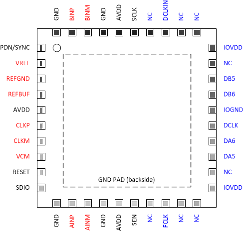
5 Pin Configuration and Functions
 Figure 5-1 RSB Package, 40-Pin WQFN
(Top View)
Table 5-1 Pin Descriptions
| PIN | I/O | Description | |
|---|---|---|---|
| Name | No. | ||
| INPUT/REFERENCE | |||
| AINP | 12 | I | Positive analog input, channel A |
| AINM | 13 | I | Negative analog input, channel A |
| BINP | 39 | I | Positive analog input, channel B |
| BINM | 38 | I | Negative analog input, channel B |
| VCM | 8 | O | Common-mode voltage output for the analog inputs, 0.95 V |
| VREF | 2 | I | External voltage reference input, 1.6 V |
| REFBUF | 4 | I | 1.2V external voltage reference input for use with internal reference buffer. Internal 100 kΩ pull-up resistor to AVDD. This pin is also used to configure default operating conditions. |
| REFGND | 3 | I | Reference ground input, 0 V |
| CLOCK | |||
| CLKP | 6 | I | Positive differential sampling clock input for the ADC |
| CLKM | 7 | I | Negative differential sampling clock input for the ADC |
| CONFIGURATION | |||
| PDN/SYNC | 1 | I | Power down/Synchronization input. This pin can be configured via the SPI interface. Active high. This pin has an internal 21 kΩ pull-down resistor. |
| RESET | 9 | I | Hardware reset. Active high. This pin has an internal 21 kΩ pull-down resistor. |
| SEN | 16 | I | Serial interface enable. Active low. This pin has an internal 21 kΩ pull-up resistor to AVDD. |
| SCLK | 35 | I | Serial interface clock input. This pin has an internal 21 kΩ pull-down resistor. |
| SDIO | 10 | I/O | Serial interface data input and output. This pin has an internal 21 kΩ pull-down resistor. |
| NC | 17,19,20,22, 29,31,32,34 | - | Do not connect |
| DIGITAL INTERFACE | |||
| DA6 | 24 | O | CMOS data output. |
| DA5 | 23 | O | CMOS data output |
| FCLK | 18 | O | CMOS frame clock output |
| DB6 | 27 | O | CMOS data output. |
| DB5 | 28 | O | CMOS data output |
| DCLKIN | 33 | I | CMOS bit clock input |
| DCLK | 25 | O | CMOS bit clock output |
| POWER SUPPLY | |||
| AVDD | 5,15,36 | I | Analog 1.8V power supply |
| GND | 11,14,37,40, PowerPad | I | Ground, 0V |
| IOVDD | 21,30 | I | 1.8V power supply for digital interface |
| IOGND | 26 | I | Ground, 0V for digital interface |