ZHCSM49 April 2021 AMC3336-Q1
PRODUCTION DATA
- 1 特性
- 2 应用
- 3 说明
- 4 Revision History
- 5 Pin Configuration and Functions
-
6 Specifications
- 6.1 Absolute Maximum Ratings
- 6.2 ESD Ratings
- 6.3 Recommended Operating Conditions
- 6.4 Thermal Information
- 6.5 Power Ratings
- 6.6 Insulation Specifications
- 6.7 Safety-Related Certifications
- 6.8 Safety Limiting Values
- 6.9 Electrical Characteristics
- 6.10 Switching Characteristics
- 6.11 Timing Diagrams
- 6.12 Insulation Characteristics Curves
- 6.13 Typical Characteristics
- 7 Detailed Description
- 8 Application and Implementation
- 9 Power Supply Recommendations
- 10Layout
- 11Device and Documentation Support
6.13 Typical Characteristics
at VDD = 3.3 V, INP = –1 V to 1 V , INN = AGND, fCLKIN = 20 MHz, sinc3 filter with OSR = 256, and 16-bit resolution (unless otherwise noted)
Figure 6-18 Integral Nonlinearity vs Temperature
Figure 6-20 Signal-to-Noise Ratio and Signal-to-Noise + Distortion vs Input Signal
Frequency
Figure 6-22 Signal-to-Noise Ratio and Signal-to-Noise + Distortion vs Supply
Voltage
Figure 6-24 Total
Harmonic Distortion vs Input Signal Amplitude
Figure 6-26 Total
Harmonic Distortion vs Clock Frequency
Figure 6-28 Total
Harmonic Distortion vs Temperature
Figure 6-30 Spurious-Free Dynamic Range vs Input Signal Frequency
Figure 6-32 Spurious-Free Dynamic Range vs Supply Voltage

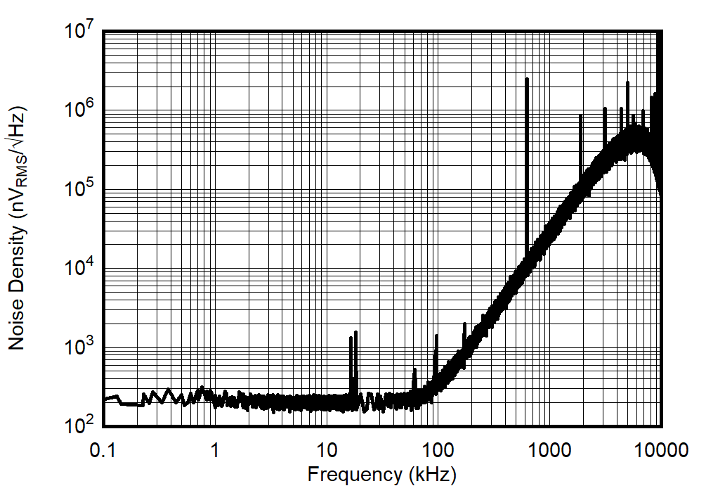
| sinc3, OSR = 1; Frequency bin-width equals 1 Hz |
| sinc3, OSR = 256, VIN = 2 VPP |
Figure 6-38 Power-Supply Rejection Ratio vs Ripple Frequency
Figure 6-40 Supply Current vs Clock Frequency
Figure 6-42 High-Side LDO Output Voltage vs Supply
Voltage
Figure 6-19 Signal-to-Noise Ratio and Signal-to-Noise + Distortion vs Input Signal
Amplitude
Figure 6-21 Signal-to-Noise Ratio and Signal-to-Noise + Distortion vs Clock
Frequency
Figure 6-23 Signal-to-Noise Ratio and Signal-to-Noise + Distortion vs
Temperature
Figure 6-25 Total
Harmonic Distortion vs Input Signal Frequency
Figure 6-27 Total
Harmonic Distortion vs Supply Voltage
Figure 6-29 Spurious-Free Dynamic Range vs Input Signal Amplitude
Figure 6-31 Spurious-Free Dynamic Range vs Clock Frequency
Figure 6-33 Spurious-Free Dynamic Range vs Temperature
| sinc3, OSR = 256, VIN = 2 VPP |
Figure 6-39 Supply Current vs Supply Voltage
Figure 6-41 Supply Current vs Temperature
Figure 6-43 IH Derating vs Ambient
Temperature