ZHCSM81A October 2020 – December 2020 TLC6C5748-Q1
PRODUCTION DATA
- 1 特性
- 2 应用
- 3 说明
- 4 Revision History
- 5 Terminal Configurations and Functions
- 6 Specifications
- 7 Parameter Measurement Information
-
8 Detailed Description
- 8.1 Overview
- 8.2 Functional Block Diagram
- 8.3 Feature Description
- 8.4 Device Functional Modes
- 9 Application and Implementation
- 10Power Supply Recommendations
- 11Layout
- 12Device and Documentation Support
- 13Mechanical, Packaging, and Orderable Information
8.3.2.2 Grayscale (GS) Data Latch
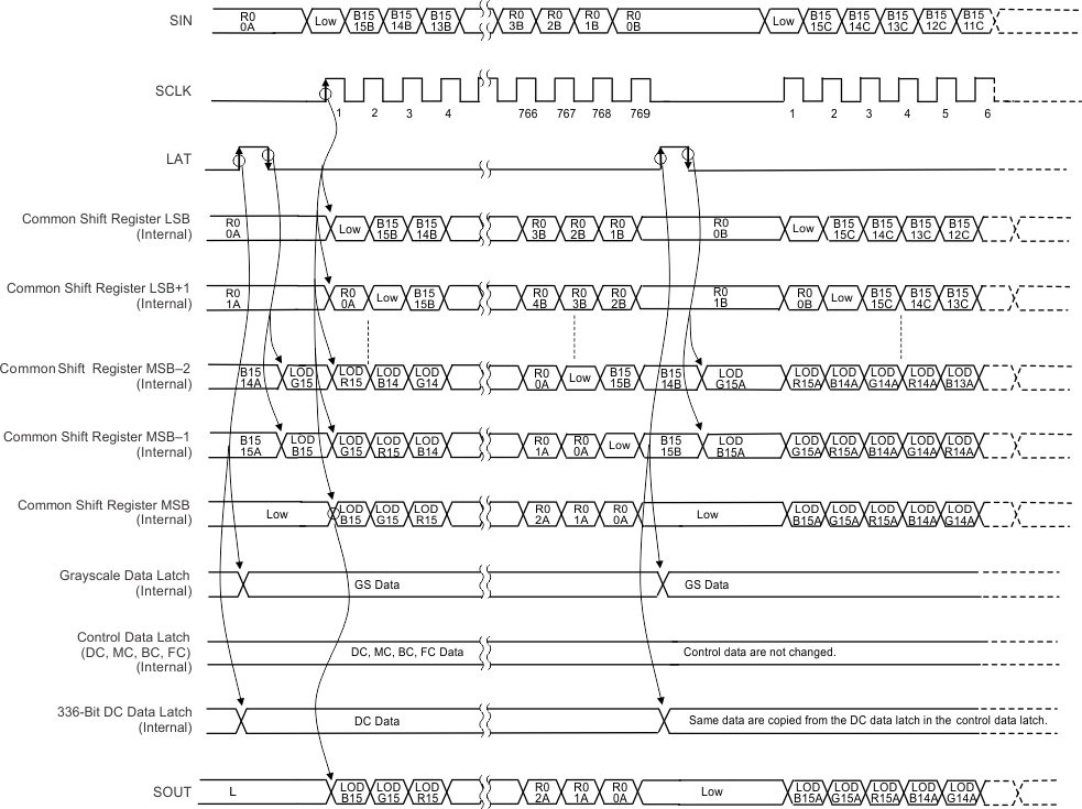
The GS data latch is 768 bits long, and sets the PWM timing for each constant-current output. The on-time of all constant-current outputs is controlled by the data in this data latch. The 768-bit GS data in the common shift register are copied to the data latch at a LAT rising edge when the common shift resister MSB is 0.
When the device is powered up, the data are random and all constant-current outputs are forced off. However, no outputs turn on until GS data are written to the GS data latch even if a GSCLK is input. The data bit assignment is shown in Table 8-1. Refer to Figure 8-2 for a GS data write timing diagram.
Table 8-1 Grayscale Data Latch Bit Description
| GS DATA LATCH BIT NUMBER | BIT NAME | DEFAULT VALUE | CONTROLLED CHANNEL | GS DATA LATCH BIT NUMBER | BIT NAME | DEFAULT VALUE | CONTROLLED CHANNEL |
|---|---|---|---|---|---|---|---|
| 15-0 | GSR0[15:0] | N/A (no default value) | Bits[15:0] for OUTR0 | 399-384 | GSR8[15:0] | N/A (no default value) | Bits[15:0] for OUTR8 |
| 31-16 | GSG0[15:0] | Bits[15:0] for OUTG0 | 415-400 | GSG8[15:0] | Bits[15:0] for OUTG8 | ||
| 47-32 | GSB0[15:0] | Bits[15:0] for OUTB0 | 431-416 | GSB8[15:0] | Bits[15:0] for OUTB8 | ||
| 63-48 | GSR1[15:0] | Bits[15:0] for OUTR1 | 447-432 | GSR9[15:0] | Bits[15:0] for OUTR9 | ||
| 79-64 | GSG1[15:0] | Bits[15:0] for OUTG1 | 463-448 | GSG9[15:0] | Bits[15:0] for OUTG9 | ||
| 95-80 | GSB1[15:0] | Bits[15:0] for OUTB1 | 479-464 | GSB9[15:0] | Bits[15:0] for OUTB9 | ||
| 111-96 | GSR2[15:0] | Bits[15:0] for OUTR2 | 495-480 | GSR10[15:0] | Bits[15:0] for OUTR10 | ||
| 127-112 | GSG2[15:0] | Bits[15:0] for OUTG2 | 511-496 | GSG10[15:0] | Bits[15:0] for OUTG10 | ||
| 143-128 | GSB2[15:0] | Bits[15:0] for OUTB2 | 527-512 | GSB10[15:0] | Bits[15:0] for OUTB10 | ||
| 159-144 | GSR3[15:0] | Bits[15:0] for OUTR3 | 543-528 | GSR11[15:0] | Bits[15:0] for OUTR11 | ||
| 175-160 | GSG3[15:0] | Bits[15:0] for OUTG3 | 559-544 | GSG11[15:0] | Bits[15:0] for OUTG11 | ||
| 191-176 | GSB3[15:0] | Bits[15:0] for OUTB3 | 575-560 | GSB11[15:0] | Bits[15:0] for OUTB11 | ||
| 207-192 | GSR4[15:0] | Bits[15:0] for OUTR4 | 591-576 | GSR12[15:0] | Bits[15:0] for OUTR12 | ||
| 223-208 | GSG4[15:0] | Bits[15:0] for OUTG4 | 607-592 | GSG12[15:0] | Bits[15:0] for OUTG12 | ||
| 239-224 | GSB4[15:0] | Bits[15:0] for OUTB4 | 623-608 | GSB12[15:0] | Bits[15:0] for OUTB12 | ||
| 255-240 | GSR5[15:0] | Bits[15:0] for OUTR5 | 639-624 | GSR13[15:0] | Bits[15:0] for OUTR13 | ||
| 271-256 | GSG5[15:0] | Bits[15:0] for OUTG5 | 655-640 | GSG13[15:0] | Bits[15:0] for OUTG13 | ||
| 287-272 | GSB5[15:0] | Bits[15:0] for OUTB5 | 671-656 | GSB13[15:0] | Bits[15:0] for OUTB13 | ||
| 303-288 | GSR6[15:0] | Bits[15:0] for OUTR6 | 687-672 | GSR14[15:0] | Bits[15:0] for OUTR14 | ||
| 319-304 | GSG6[15:0] | Bits[15:0] for OUTG6 | 703-688 | GSG14[15:0] | Bits[15:0] for OUTG14 | ||
| 335-320 | GSB6[15:0] | Bits[15:0] for OUTB6 | 719-704 | GSB14[15:0] | Bits[15:0] for OUTB14 | ||
| 351-336 | GSR7[15:0] | Bits[15:0] for OUTR7 | 735-720 | GSR15[15:0] | Bits[15:0] for OUTR15 | ||
| 367-352 | GSG7[15:0] | Bits[15:0] for OUTG7 | 751-736 | GSG15[15:0] | Bits[15:0] for OUTG15 | ||
| 383-368 | GSB7[15:0] | Bits[15:0] for OUTB7 | 767-752 | GSB15[15:0] | Bits[15:0] for OUTB15 |
 Figure 8-2 Grayscale Data Write Timing Diagram (RFRESH = 0)