ZHCSM81A October   2020  – December 2020 TLC6C5748-Q1

PRODUCTION DATA  

  1. 特性
  2. 应用
  3. 说明
  4. Revision History
  5. Terminal Configurations and Functions
  6. Specifications
    1. 6.1 Absolute Maximum Ratings
    2. 6.2 ESD Ratings
    3. 6.3 Recommended Operating Conditions
    4. 6.4 Thermal Information
    5. 6.5 Electrical Characteristics
    6. 6.6 Switching Characteristics
    7. 6.7 Typical Characteristics
  7. Parameter Measurement Information
    1. 7.1 Terminal-Equivalent Input and Output Schematic Diagrams
    2. 7.2 Test Circuits
    3. 7.3 Timing Diagrams
  8. Detailed Description
    1. 8.1 Overview
    2. 8.2 Functional Block Diagram
    3. 8.3 Feature Description
      1. 8.3.1 Output Current Calculation
      2. 8.3.2 Register and Data Latch Configuration
        1. 8.3.2.1 769-Bit Common Shift Register
        2. 8.3.2.2 Grayscale (GS) Data Latch
        3. 8.3.2.3 Control Data Latch
        4. 8.3.2.4 Dot Correction (DC) Data Latch
        5. 8.3.2.5 Maximum Current (MC) Data Latch
        6. 8.3.2.6 Global Brightness Control (BC) Data Latch
        7. 8.3.2.7 Function Control (FC) Data Latch
      3. 8.3.3 Status Information Data (SID)
      4. 8.3.4 LED Open Detection (LOD)
      5. 8.3.5 LED Short Detection (LSD)
      6. 8.3.6 Thermal Shutdown Faults (TSD)
      7. 8.3.7 Noise Reduction
    4. 8.4 Device Functional Modes
      1. 8.4.1 Maximum Current Control (MC) Function
      2. 8.4.2 Dot Correction (DC) Function
      3. 8.4.3 Global Brightness Control (BC) Function
      4. 8.4.4 Grayscale (GS) Function (PWM Control)
        1. 8.4.4.1 Conventional PWM Control
        2. 8.4.4.2 Enhanced Spectrum (ES) PWM Control
        3. 8.4.4.3 Auto Display Repeat Function
        4. 8.4.4.4 Display Timing Reset Function
        5. 8.4.4.5 Auto Data Refresh Function
  9. Application and Implementation
    1. 9.1 Application Information
    2. 9.2 Typical Application
      1. 9.2.1 Daisy-Chain Application
        1. 9.2.1.1 Design Requirements
        2. 9.2.1.2 Detailed Design Procedure
          1. 9.2.1.2.1 Step-by-Step Design Procedure
          2. 9.2.1.2.2 Maximum Current (MC) Data
          3. 9.2.1.2.3 Global Brightness Control (BC) Data
          4. 9.2.1.2.4 Dot Correction (DC) Data
          5. 9.2.1.2.5 Grayscale (GS) Data
          6. 9.2.1.2.6 Other Control Data
        3. 9.2.1.3 Application Curves
  10. 10Power Supply Recommendations
  11. 11Layout
    1. 11.1 Layout Guidelines
    2. 11.2 Layout Example
  12. 12Device and Documentation Support
    1. 12.1 接收文档更新通知
    2. 12.2 支持资源
    3. 12.3 Trademarks
    4. 12.4 静电放电警告
    5. 12.5 术语表
  13. 13Mechanical, Packaging, and Orderable Information

Typical Characteristics

At TA = +25°C and VCC = 5.0 V, unless otherwise noted.
GUID-BD1E1FFB-8648-435E-9DC9-7970BF9FF91B-low.png
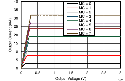
BCX = DCXn = 7Fh
Figure 6-1 Output Current vs Output Voltage (MCX Changing)
GUID-C394663F-FDAA-4227-BCE9-6746945AC729-low.png
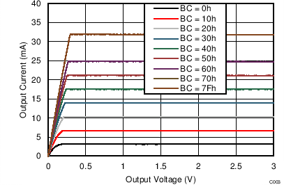
BCX = DCXn = 7Fh
Figure 6-3 Output Current vs Output Voltage (BCX Changing)
GUID-2A15B9D8-490C-475C-9FE6-8661F5ED8428-low.png
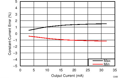
BCX = DCXn = 7Fh VOUTXn = 0.8 V
Figure 6-5 Constant-Current Error vs Output Current (Channel-to-Channel in Each Color Group)
GUID-82C6549F-0C0D-425C-AD82-EAC65AF8E5DB-low.png
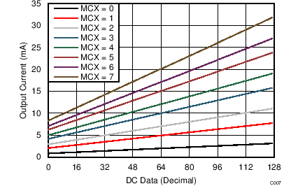
BCX = 7Fh VOUTXn = 0.8 V
Figure 6-7 Dot Correction (DC) Linearity
GUID-3532C67A-32E8-4245-9ECB-88DC90D280D5-low.png
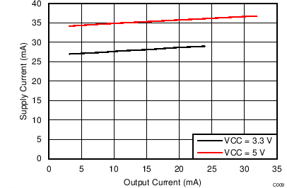
BCX = DCXn = 7Fh SIN = 12.5 MHz SCLK = 25 MHz
GSCLK = 33 MHz VOUT = 0.8 V GSXn = FFFFh
Figure 6-9 Supply Current vs Output Current
GUID-EF891618-6F6F-49C6-8C46-144841677823-low.gif
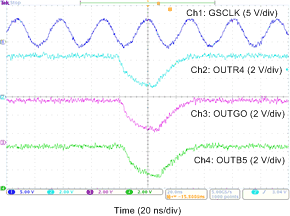
MCX = 7 BCX = DCXn = 7Fh GSCLK = 33 MHz
VLED = 4.5 V RL = 120 Ω GSXn = 0001h
Figure 6-11 Constant-Current Output Voltage Waveform
GUID-E9B42EC0-4FE4-4421-B1D1-7BF53717D87F-low.png
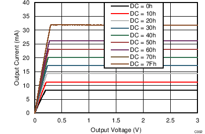
BCX = DCXn = 7Fh
Figure 6-2 Output Current vs Output Voltage (DCXn Changing)
GUID-A5842E23-9FF4-4B65-8F6E-353E1169D9DC-low.png
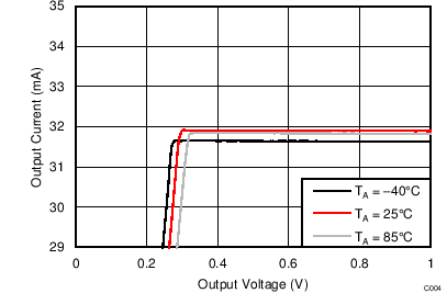
BCX = DCXn = 7Fh
Figure 6-4 Output Current vs Output Voltage (Temperature Changing)
GUID-59E9EC3A-A58F-4B16-B82F-0B7EB16AF581-low.png
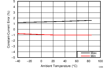
MCX = 4 BCX = DCXn = 7Fh VOUTXn = 0.8 V
Figure 6-6 Constant-Current Error vs Ambient Temperature (Channel-to-Channel in Each Color Group)
GUID-69CA08E9-D9F4-414E-B59B-E2FAB77F082F-low.png
DCXn = 7Fh VOUTXn = 0.8 V
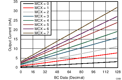
Figure 6-8 Global Brightness Control (BC) Linearity
GUID-17D91E45-08EB-4E04-8FFB-DD902B12DDEB-low.png
MCX = 4 BCX = DCXn = 7Fh SIN = 12.5 MHz
SCLK = 25 MHz GSCLK = 33 MHz VOUT = 0.8 V
GSXn = FFFFh
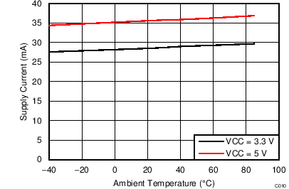
Figure 6-10 Supply Current vs Ambient Temperature