ZHCSM81A October   2020  – December 2020 TLC6C5748-Q1

PRODUCTION DATA  

  1. 特性
  2. 应用
  3. 说明
  4. Revision History
  5. Terminal Configurations and Functions
  6. Specifications
    1. 6.1 Absolute Maximum Ratings
    2. 6.2 ESD Ratings
    3. 6.3 Recommended Operating Conditions
    4. 6.4 Thermal Information
    5. 6.5 Electrical Characteristics
    6. 6.6 Switching Characteristics
    7. 6.7 Typical Characteristics
  7. Parameter Measurement Information
    1. 7.1 Terminal-Equivalent Input and Output Schematic Diagrams
    2. 7.2 Test Circuits
    3. 7.3 Timing Diagrams
  8. Detailed Description
    1. 8.1 Overview
    2. 8.2 Functional Block Diagram
    3. 8.3 Feature Description
      1. 8.3.1 Output Current Calculation
      2. 8.3.2 Register and Data Latch Configuration
        1. 8.3.2.1 769-Bit Common Shift Register
        2. 8.3.2.2 Grayscale (GS) Data Latch
        3. 8.3.2.3 Control Data Latch
        4. 8.3.2.4 Dot Correction (DC) Data Latch
        5. 8.3.2.5 Maximum Current (MC) Data Latch
        6. 8.3.2.6 Global Brightness Control (BC) Data Latch
        7. 8.3.2.7 Function Control (FC) Data Latch
      3. 8.3.3 Status Information Data (SID)
      4. 8.3.4 LED Open Detection (LOD)
      5. 8.3.5 LED Short Detection (LSD)
      6. 8.3.6 Thermal Shutdown Faults (TSD)
      7. 8.3.7 Noise Reduction
    4. 8.4 Device Functional Modes
      1. 8.4.1 Maximum Current Control (MC) Function
      2. 8.4.2 Dot Correction (DC) Function
      3. 8.4.3 Global Brightness Control (BC) Function
      4. 8.4.4 Grayscale (GS) Function (PWM Control)
        1. 8.4.4.1 Conventional PWM Control
        2. 8.4.4.2 Enhanced Spectrum (ES) PWM Control
        3. 8.4.4.3 Auto Display Repeat Function
        4. 8.4.4.4 Display Timing Reset Function
        5. 8.4.4.5 Auto Data Refresh Function
  9. Application and Implementation
    1. 9.1 Application Information
    2. 9.2 Typical Application
      1. 9.2.1 Daisy-Chain Application
        1. 9.2.1.1 Design Requirements
        2. 9.2.1.2 Detailed Design Procedure
          1. 9.2.1.2.1 Step-by-Step Design Procedure
          2. 9.2.1.2.2 Maximum Current (MC) Data
          3. 9.2.1.2.3 Global Brightness Control (BC) Data
          4. 9.2.1.2.4 Dot Correction (DC) Data
          5. 9.2.1.2.5 Grayscale (GS) Data
          6. 9.2.1.2.6 Other Control Data
        3. 9.2.1.3 Application Curves
  10. 10Power Supply Recommendations
  11. 11Layout
    1. 11.1 Layout Guidelines
    2. 11.2 Layout Example
  12. 12Device and Documentation Support
    1. 12.1 接收文档更新通知
    2. 12.2 支持资源
    3. 12.3 Trademarks
    4. 12.4 静电放电警告
    5. 12.5 术语表
  13. 13Mechanical, Packaging, and Orderable Information

LED Short Detection (LSD)

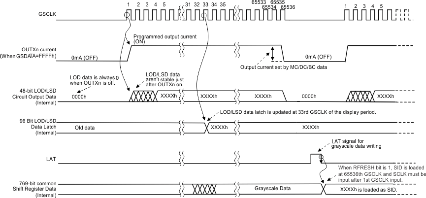
LSD data detect a fault caused by a shorted LED between LED terminals by comparing the OUTXn voltage to the LSD detection threshold voltage level set by LSDVLT in the control data latch. If the OUTXn voltage is higher than the programmed voltage when OUTXn is on, the corresponding output LSD bit is set to 1 to indicate a shorted LED. Otherwise, the LSD bit is set to 0. LSD data are only valid for outputs that are programmed to be on. LSD data are latched into the LOD, LSD data latch at the 33rd GSCLK. LSD data for outputs programmed to be off at the 33rd GSCLK are always 0. The LSD open detection circuit is shown in Figure 8-5 and Table 8-7 lists an LSD truth table. Refer to Figure 8-6 for an LSD read timing diagram.
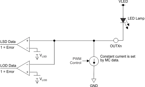
GUID-B835FCFA-A4D3-4E9E-A6EA-DBB305984712-low.gifFigure 8-5 LOD and LSD Circuit
Table 8-7 LOD and LSD Truth Table
SID DATACONDITION
LODLSD
0LED is not opened (VOUTXn > VLOD)LED is not shorted (VOUTXn ≤ VLSD)
1LED is open or shorted to GND (VOUTXn ≤ VLOD)LED is shorted between anode and cathode, or shorted to higher voltage side (VOUTXn > VLSD)
GUID-C059D4E5-5235-480D-BE60-A0904AD65C32-low.gifFigure 8-6 LOD and LSD Read and Load Timing Diagram