ZHCSM81A October 2020 – December 2020 TLC6C5748-Q1
PRODUCTION DATA
- 1 特性
- 2 应用
- 3 说明
- 4 Revision History
- 5 Terminal Configurations and Functions
- 6 Specifications
- 7 Parameter Measurement Information
-
8 Detailed Description
- 8.1 Overview
- 8.2 Functional Block Diagram
- 8.3 Feature Description
- 8.4 Device Functional Modes
- 9 Application and Implementation
- 10Power Supply Recommendations
- 11Layout
- 12Device and Documentation Support
- 13Mechanical, Packaging, and Orderable Information
8.4.4.4 Display Timing Reset Function
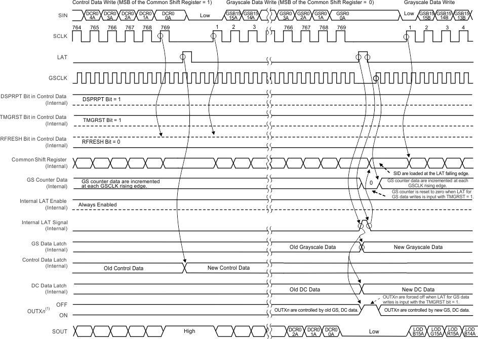
The display timing reset function allows initializing the display timing with a LAT rising edge. This function can be switched on or off with the TMGRST bit in the control data latch. When the TMGRST bit is 1, the GS counter is reset to 0 and all outputs are forced off at the LAT rising edge for a GS data write. Furthermore, the 768-bit GS data latch is updated with the data from the common shift register and the 336-bit DC data latch is updated with the DC data in the 371-bit control data latch. When the TMGRST bit is 0, the GS counter is not reset and the outputs are not forced off, even if a LAT rising edge is input. A timing diagram for this function is shown in Figure 8-10.
 Figure 8-10 Display Timing Reset Function (DSPRPT = 1, TMGRST = 1, and RFRESH = 0)