ZHCSMI7A December 2020 – May 2021 TPS92633-Q1
PRODUCTION DATA
- 1 特性
- 2 应用
- 3 说明
- 4 Revision History
- 5 Pin Configuration and Functions
- 6 Specifications
-
7 Detailed Description
- 7.1 Overview
- 7.2 Functional Block Diagram
- 7.3
Feature Description
- 7.3.1 Power Supply (SUPPLY)
- 7.3.2 Enable and Shutdown (EN)
- 7.3.3 Reference Current (IREF)
- 7.3.4 Constant-Current Output and Setting (INx)
- 7.3.5 Analog Current Control (ICTRL)
- 7.3.6 Thermal Sharing Resistor (OUTx and RESx)
- 7.3.7 PWM Control (PWMx)
- 7.3.8 Supply Control
- 7.3.9
Diagnostics
- 7.3.9.1 IREF Short-to-GND Detection
- 7.3.9.2 IREF Open Detection
- 7.3.9.3 LED Short-to-GND Detection
- 7.3.9.4 LED Open-Circuit Detection
- 7.3.9.5 Single LED Short-Circuit Detection (SLS_REF)
- 7.3.9.6 LED Open-Circuit and Single LED Short-Circuit Detection Enable (DIAGEN)
- 7.3.9.7 Low Dropout Operation
- 7.3.9.8 Over-Temperature Protection
- 7.3.10 FAULT Bus Output With One-Fails–All-Fail
- 7.3.11 FAULT Table
- 7.3.12 LED Fault Summary
- 7.3.13 IO Pins Inner Connection
- 7.4 Device Functional Modes
- 8 Application and Implementation
- 9 Power Supply Recommendations
- 10Layout
- 11Device and Documentation Support
- 12Mechanical, Packaging, and Orderable Information
7.3.5.1 Off-Board Brightness Binning Resistor
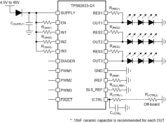
With analog current control feature, a LED brightness binning resistor can be connected to ICTRL pin to set the output current according to LED brightness bin. The binning resistor can be placed in off-board with LED units. In order to achieve the best performance for the noise rejection, two resistors in serial can be adopted. One resistor is placed as closed as possible to the ICTRL pin in the same PCB board with device, and another one real binning resistor is placed in the other PCB board with LED units together.
As Figure 7-1 illustrated, the R(ICTRL1) resistor and C(ICTRL) ceramic capacitor need to be placed as close as possible to the ICTRL pin for noise decoupling. The off-board R(ICTRL2) resistor can be placed in LED board as real binning resistor. TI recommends a 10-nF ceramic capacitor for C(ICTRL).
 Figure 7-1 Application
Schematic For Off-Board Brightness Binning Resistor
Figure 7-1 Application
Schematic For Off-Board Brightness Binning ResistorThe V(CS_REG) is 50 mV typically when the ICTRL pin is short to GND.