ZHCSMK3B November   2020  – November 2021 ADS131B04-Q1

PRODUCTION DATA  

  1. 特性
  2. 应用
  3. 说明
  4. Revision History
  5. Pin Configuration and Functions
  6. Specifications
    1. 6.1 Absolute Maximum Ratings
    2. 6.2 ESD Ratings
    3. 6.3 Recommended Operating Conditions
    4. 6.4 Thermal Information
    5. 6.5 Electrical Characteristics
    6. 6.6 Timing Requirements
    7. 6.7 Switching Characteristics
    8. 6.8 Timing Diagrams
    9. 6.9 Typical Characteristics
  7. Parameter Measurement Information
    1. 7.1 Noise Measurements
  8. Detailed Description
    1. 8.1 Overview
    2. 8.2 Functional Block Diagram
    3. 8.3 Feature Description
      1. 8.3.1  Input ESD Protection Circuitry
      2. 8.3.2  Input Multiplexer
      3. 8.3.3  Programmable Gain Amplifier (PGA)
      4. 8.3.4  Voltage Reference
      5. 8.3.5  Internal Test Signals
      6. 8.3.6  Clocking
        1. 8.3.6.1 External Clock Using CLKIN Pin
        2. 8.3.6.2 Internal Oscillator
      7. 8.3.7  ΔΣ Modulator
      8. 8.3.8  Digital Filter
        1. 8.3.8.1 Digital Filter Implementation
          1. 8.3.8.1.1 Fast-Settling Filter
          2. 8.3.8.1.2 SINC3 and SINC3 + SINC1 Filter
        2. 8.3.8.2 Digital Filter Characteristic
      9. 8.3.9  Calibration Registers
      10. 8.3.10 Register Map CRC
    4. 8.4 Device Functional Modes
      1. 8.4.1 Power-Up and Reset
        1. 8.4.1.1 Power-On Reset
        2. 8.4.1.2 SYNC/RESET Pin
        3. 8.4.1.3 RESET Command
      2. 8.4.2 Fast Start-Up Behavior
      3. 8.4.3 Conversion Modes
        1. 8.4.3.1 Continuous-Conversion Mode
        2. 8.4.3.2 Global-Chop Mode
      4. 8.4.4 Power Modes
      5. 8.4.5 Standby Mode
      6. 8.4.6 Synchronization
    5. 8.5 Programming
      1. 8.5.1 Serial Interface
        1. 8.5.1.1  Chip Select (CS)
        2. 8.5.1.2  Serial Data Clock (SCLK)
        3. 8.5.1.3  Serial Data Input (DIN)
        4. 8.5.1.4  Serial Data Output (DOUT)
        5. 8.5.1.5  Data Ready (DRDY)
        6. 8.5.1.6  SPI Communication Frames
        7. 8.5.1.7  SPI Communication Words
        8. 8.5.1.8  Short SPI Frames
        9. 8.5.1.9  Communication Cyclic Redundancy Check (CRC)
        10. 8.5.1.10 SPI Timeout
      2. 8.5.2 ADC Conversion Data Format
      3. 8.5.3 Commands
        1. 8.5.3.1 NULL (0000 0000 0000 0000)
        2. 8.5.3.2 RESET (0000 0000 0001 0001)
        3. 8.5.3.3 STANDBY (0000 0000 0010 0010)
        4. 8.5.3.4 WAKEUP (0000 0000 0011 0011)
        5. 8.5.3.5 LOCK (0000 0101 0101 0101)
        6. 8.5.3.6 UNLOCK (0000 0110 0110 0110)
        7. 8.5.3.7 RREG (101a aaaa annn nnnn)
          1. 8.5.3.7.1 Reading a Single Register
          2. 8.5.3.7.2 Reading Multiple Registers
        8. 8.5.3.8 WREG (011a aaaa annn nnnn)
      4. 8.5.4 Collecting Data for the First Time or After a Pause in Data Collection
    6. 8.6 Register Map
  9. Application and Implementation
    1. 9.1 Application Information
      1. 9.1.1 Troubleshooting
      2. 9.1.2 Unused Inputs and Outputs
      3. 9.1.3 Antialias Filter
      4. 9.1.4 Minimum Interface Connections
      5. 9.1.5 Multiple Device Configuration
    2. 9.2 Typical Application
      1. 9.2.1 Design Requirements
      2. 9.2.2 Detailed Design Procedure
        1. 9.2.2.1 Current Shunt Measurement
        2. 9.2.2.2 Battery Pack Voltage Measurement
        3. 9.2.2.3 Shunt Temperature Measurement
        4. 9.2.2.4 Auxiliary Analog Supply Voltage Measurement
      3. 9.2.3 Application Curves
  10. 10Power Supply Recommendations
    1. 10.1 CAP Pin Capacitor Requirement
    2. 10.2 Power-Supply Sequencing
    3. 10.3 Power-Supply Decoupling
  11. 11Layout
    1. 11.1 Layout Guidelines
    2. 11.2 Layout Example
  12. 12Device and Documentation Support
    1. 12.1 Documentation Support
      1. 12.1.1 Related Documentation
    2. 12.2 Receiving Notification of Documentation Updates
    3. 12.3 支持资源
    4. 12.4 Trademarks
    5. 12.5 Electrostatic Discharge Caution
    6. 12.6 术语表
  13. 13Mechanical, Packaging, and Orderable Information

Minimum Interface Connections

Figure 9-2 depicts how the ADS131B04-Q1 can be configured for the minimum number of interface pins. This configuration is useful when using data isolation to minimize the number of isolation channels required or when the microcontroller (MCU) pins are limited.

The CLKIN pin requires an LVCMOS clock that can be either generated by the MCU or created using a local LVCMOS output oscillator when the device is configured for use with an external clock. Otherwise tie the CLKIN pin to DGND if the internal oscillator is used. Tie the SYNC/RESET pin to DVDD in hardware if unused. The DRDY pin can be left floating if unused. Connect either SYNC/RESET or DRDY to the MCU to make sure the MCU stays synchronized to ADC conversions. If the MCU provides CLKIN, the CLKIN periods can be counted to determine the sample period rather than forcing synchronization using the SYNC/RESET pin or monitoring the DRDY pin. Synchronization cannot be regained if a bit error occurs on the clock and samples can be missed if the SYNC/RESET or DRDY pins are not used. CS can be tied low in hardware if the ADS131B04-Q1 is the only device on the SPI bus. Make sure the data input and output CRC are enabled and are used to guard against faulty register reads and writes if CS is tied low permanently.
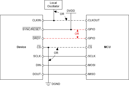
GUID-20201021-CA0I-11MC-6W4Z-NZNZMMHKVVKG-low.gif Figure 9-2 Minimum Connections Required to Operate the ADS131B04-Q1