ZHCSMM8A December 2020 – June 2021 TLV320ADC3120
PRODUCTION DATA
- 1 特性
- 2 应用
- 3 说明
- 4 Revision History
- 5 Device Comparison Table
- 6 Pin Configuration and Functions
-
7 Specifications
- 7.1 Absolute Maximum Ratings
- 7.2 ESD Ratings
- 7.3 Recommended Operating Conditions
- 7.4 Thermal Information
- 7.5 Electrical Characteristics
- 7.6 Timing Requirements: I2C Interface
- 7.7 Switching Characteristics: I2C Interface
- 7.8 Timing Requirements: TDM, I2S or LJ Interface
- 7.9 Switching Characteristics: TDM, I2S or LJ Interface
- 7.10 Timing Requirements: PDM Digital Microphone Interface
- 7.11 Switching Characteristics: PDM Digital Microphone Interface
- 7.12 Timing Diagrams
- 7.13 Typical Characteristics
-
8 Detailed Description
- 8.1 Overview
- 8.2 Functional Block Diagram
- 8.3
Feature Description
- 8.3.1 Serial Interfaces
- 8.3.2 Phase-Locked Loop (PLL) and Clock Generation
- 8.3.3 Input Channel Configurations
- 8.3.4 Reference Voltage
- 8.3.5 Programmable Microphone Bias
- 8.3.6
Signal-Chain Processing
- 8.3.6.1 Programmable Channel Gain and Digital Volume Control
- 8.3.6.2 Programmable Channel Gain Calibration
- 8.3.6.3 Programmable Channel Phase Calibration
- 8.3.6.4 Programmable Digital High-Pass Filter
- 8.3.6.5 Programmable Digital Biquad Filters
- 8.3.6.6 Programmable Channel Summer and Digital Mixer
- 8.3.6.7
Configurable Digital Decimation Filters
- 8.3.6.7.1
Linear Phase Filters
- 8.3.6.7.1.1 Sampling Rate: 7.35 kHz to 8 kHz
- 8.3.6.7.1.2 Sampling Rate: 14.7 kHz to 16 kHz
- 8.3.6.7.1.3 Sampling Rate: 22.05 kHz to 24 kHz
- 8.3.6.7.1.4 Sampling Rate: 29.4 kHz to 32 kHz
- 8.3.6.7.1.5 Sampling Rate: 44.1 kHz to 48 kHz
- 8.3.6.7.1.6 Sampling Rate: 88.2 kHz to 96 kHz
- 8.3.6.7.1.7 Sampling Rate: 176.4 kHz to 192 kHz
- 8.3.6.7.1.8 Sampling Rate: 352.8 kHz to 384 kHz
- 8.3.6.7.1.9 Sampling Rate: 705.6 kHz to 768 kHz
- 8.3.6.7.2 Low-Latency Filters
- 8.3.6.7.3
Ultra-Low Latency Filters
- 8.3.6.7.3.1 Sampling Rate: 14.7 kHz to 16 kHz
- 8.3.6.7.3.2 Sampling Rate: 22.05 kHz to 24 kHz
- 8.3.6.7.3.3 Sampling Rate: 29.4 kHz to 32 kHz
- 8.3.6.7.3.4 Sampling Rate: 44.1 kHz to 48 kHz
- 8.3.6.7.3.5 Sampling Rate: 88.2 kHz to 96 kHz
- 8.3.6.7.3.6 Sampling Rate: 176.4 kHz to 192 kHz
- 8.3.6.7.3.7 Sampling Rate: 352.8 kHz to 384 kHz
- 8.3.6.7.1
Linear Phase Filters
- 8.3.7 Automatic Gain Controller (AGC)
- 8.3.8 Voice Activity Detection (VAD)
- 8.3.9 Digital PDM Microphone Record Channel
- 8.3.10 Interrupts, Status, and Digital I/O Pin Multiplexing
- 8.4 Device Functional Modes
- 8.5 Programming
- 8.6 Register Maps
- 9 Application and Implementation
- 10Power Supply Recommendations
- 11Layout
- 12Device and Documentation Support
- 13Mechanical, Packaging, and Orderable Information
8.3.6 Signal-Chain Processing
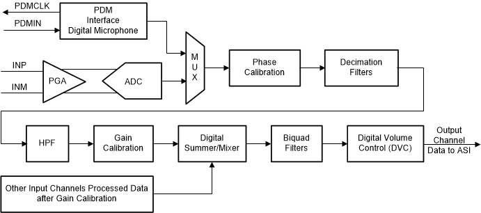
The TLV320ADC3120 signal chain is comprised of very-low-noise, high-performance, and low-power analog blocks and highly flexible and programmable digital processing blocks. The high performance and flexibility combined with a compact package makes the TLV320ADC3120 optimized for a variety of end-equipments and applications that require multichannel audio capture. Figure 8-16 shows a conceptual block diagram that highlights the various building blocks used in the signal chain, and how the blocks interact in the signal chain.
 Figure 8-16 Signal-Chain Processing Flowchart
The front-end PGA is very low noise, with a 120-dB dynamic range performance. Along with a low-noise and low-distortion, multibit, delta-sigma ADC, the front-end PGA enables the TLV320ADC3120 to record a far-field audio signal with very high fidelity, both in quiet and loud environments. Moreover, the ADC architecture has inherent antialias filtering with a high rejection of out-of-band frequency noise around multiple modulator frequency components. Therefore, the device prevents noise from aliasing into the audio band during ADC sampling. Further on in the signal chain, an integrated, high-performance multistage digital decimation filter sharply cuts off any out-of-band frequency noise with high stop-band attenuation.
The device also has an integrated programmable biquad filter that allows for custom low-pass, high-pass, or any other desired frequency shaping. Thus, the overall signal chain architecture removes the requirement to add external components for antialiasing low-pass filtering, and thus saves drastically on the external system component cost and board space. See the TLV320ADCx140 Integrated Analog Anti-Aliasing Filter and Flexible Digital Filter application report for further details.
The signal chain also consists of various highly programmable digital processing blocks such as phase calibration, gain calibration, high-pass filter, digital summer or mixer, biquad filters, and volume control. The details on these processing blocks are discussed further in this section. The device also supports up to four digital PDM microphone recording channels when the analog record channels are not used. Channels 1 to 2 in the signal chain block diagram of Figure 8-16 are as described in this section, however, channels 3 to 4 only support the digital microphone recording option and do not support the digital summer or mixer option.
The desired input channels for recording can be enabled or disabled by using the IN_CH_EN (P0_R115) register, and the output channels for the audio serial interface can be enabled or disabled by using the ASI_OUT_EN (P0_R116) register. In general, the device supports simultaneous power-up and power-down of all active channels for simultaneous recording. However, based on the application needs, if some channels must be powered-up or powered-down dynamically when the other channel recording is on, then that use case is supported by setting the DYN_CH_PUPD_EN (P0_R117_D4) register bit to 1'b1.
The device supports an input signal bandwidth up to 80 kHz, which allows the high-frequency non-audio signal to be recorded by using a 176.4-kHz (or higher) sample rate.
For output sample rates of 48 kHz or lower, the device supports all features for 4-channel recording and various programmable processing blocks. However, for output sample rates higher than 48 kHz, there are limitations in the number of simultaneous channel recordings supported and the number of biquad filters and such. See the TLV320ADCx140 Sampling Rates and Programmable Processing Blocks Supported application report for further details.