ZHCSMR7C November 2020 – July 2022 AWR6843AOP
PRODUCTION DATA
- 1 特性
- 2 应用
- 3 说明
- 4 功能方框图
- 5 Revision History
- 6 Device Comparison
- 7 Terminal Configuration and Functions
-
8 Specifications
- 8.1 Absolute Maximum Ratings
- 8.2 ESD Ratings
- 8.3 Power-On Hours (POH)
- 8.4 Recommended Operating Conditions
- 8.5 Power Supply Specifications
- 8.6 Power Consumption Summary
- 8.7 RF Specification
- 8.8 CPU Specifications
- 8.9 Thermal Resistance Characteristics for FCBGA Package [ALP0180A]
- 8.10
Timing and Switching Characteristics
- 8.10.1 Antenna Radiation Patterns
- 8.10.2 Antenna Positions
- 8.10.3 Power Supply Sequencing and Reset Timing
- 8.10.4 Input Clocks and Oscillators
- 8.10.5 Multibuffered / Standard Serial Peripheral Interface (MibSPI)
- 8.10.6 LVDS Interface Configuration
- 8.10.7 General-Purpose Input/Output
- 8.10.8 Controller Area Network - Flexible Data-rate (CAN-FD)
- 8.10.9 Serial Communication Interface (SCI)
- 8.10.10 Inter-Integrated Circuit Interface (I2C)
- 8.10.11 Quad Serial Peripheral Interface (QSPI)
- 8.10.12 ETM Trace Interface
- 8.10.13 Data Modification Module (DMM)
- 8.10.14 JTAG Interface
- 9 Detailed Description
- 10Monitoring and Diagnostics
- 11Applications, Implementation, and Layout
- 12Device and Documentation Support
- 13Mechanical, Packaging, and Orderable Information
9.3.2 Processor Subsystem
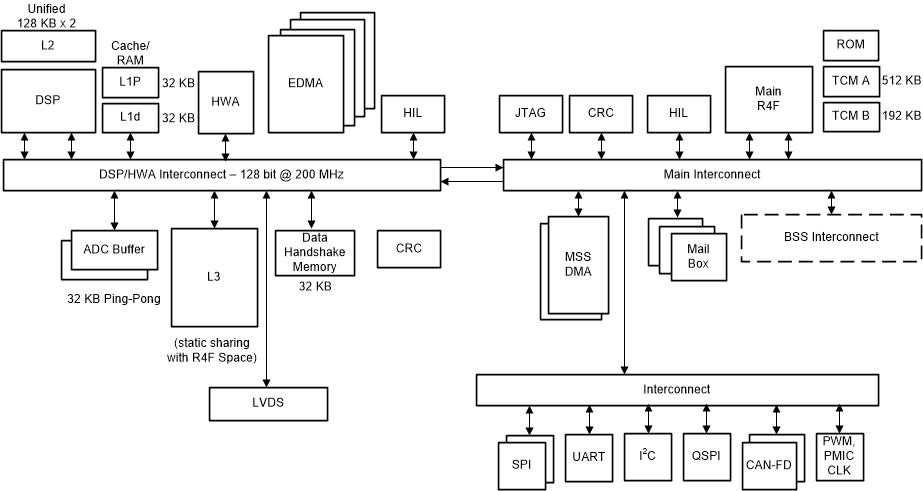
 Figure 9-5 Processor Subsystem
Figure 9-5shows the block diagram for customer programmable processor subsystems in the AWR6843AOP device. At a high level there are two customer programmable subsystems, as shown separated by a dotted line in the diagram. Left hand side shows the DSP Subsystem which contains TI's high-performance C674x DSP, hardware accelerator, a high-bandwidth interconnect for high performance (128-bit, 200MHz), and associated peripherals – four DMAs for data transfer,
LVDS interface for Measurement data output, L3 Radar data cube memory, ADC buffers, CRC engine, and data handshake memory (additional memory provided on interconnect).
The C674x DSP and L1/L2 RAM portion of the DSP subsystem is not supported on the AWR6443 device and therefore, the available memory is 1.4MB compared to 1.75MB on the IWR6843 device. For more information on the features supported and not supported on each device, see the Device Features Comparison table.
The right side of the diagram shows the main subsystem. Main subsystem as the name suggests is the centre of the device and controls all the device peripherals and house-keeping activities of the device. Main subsystem contains Cortex-R4F (Main R4F) processor and associated peripherals and house-keeping components such as DMAs, CRC and Peripherals (I2C, UART, SPIs, CAN-FD, PMIC clocking module, PWM, and others) connected to Main Interconnect through Peripheral Central Resource (PCR interconnect).
Details of the DSP CPU core can be found at http://www.ti.com/product/TMS320C6748.
HIL module is shown in both the subsystems and can be used to perform the radar operations feeding the captured data from outside into the device without involving the RF subsystem. HIL on main SS is for controlling the configuration and HIL on DSPSS for high speed ADC data input to the device. Both HIL modules uses the same IOs on the device, one additional IO (DMM_MUX_IN) allows selecting either of the two.