ZHCSN67N July   1997  – April 2021 SN55LVDS31 , SN65LVDS31 , SN65LVDS3487 , SN65LVDS9638

PRODUCTION DATA  

  1. 特性
  2. 应用
  3. 说明
  4. Revision History
  5. 说明(续)
  6. Pin Configuration and Functions
  7. Specifications
    1. 7.1 Absolute Maximum Ratings (1)
    2. 7.2 ESD Ratings
    3. 7.3 Recommended Operating Conditions
    4. 7.4 Thermal Information
    5. 7.5 Electrical Characteristics: SN55LVDS31
    6. 7.6 Electrical Characteristics: SN65LVDSxxxx
    7. 7.7 Switching Characteristics: SN55LVDS31
    8. 7.8 Switching Characteristics: SN65LVDSxxxx
    9. 7.9 Typical Characteristics
      1. 7.9.1 17
  8. Parameter Measurement Information
    1. 8.1 19
  9. Detailed Description
    1. 9.1 Overview
    2. 9.2 Functional Block Diagram
    3. 9.3 Feature Description
      1. 9.3.1 Driver Disabled Output
      2. 9.3.2 NC Pins
      3. 9.3.3 Unused Enable Pins
      4. 9.3.4 Driver Equivalent Schematics
    4. 9.4 Device Functional Modes
  10. 10Application and Implementation
    1. 10.1 Application Information
    2. 10.2 Typical Application
      1. 10.2.1 Point-to-Point Communications
        1. 10.2.1.1 Design Requirements
        2. 10.2.1.2 Detailed Design Procedure
          1. 10.2.1.2.1 Driver Supply Voltage
          2. 10.2.1.2.2 Driver Bypass Capacitance
          3. 10.2.1.2.3 Driver Output Voltage
          4. 10.2.1.2.4 Interconnecting Media
          5. 10.2.1.2.5 PCB Transmission Lines
          6. 10.2.1.2.6 Termination Resistor
          7. 10.2.1.2.7 Driver NC Pins
        3. 10.2.1.3 Application Curve
      2. 10.2.2 Multidrop Communications
        1. 10.2.2.1 Design Requirements
        2. 10.2.2.2 Detailed Design Procedure
          1. 10.2.2.2.1 Interconnecting Media
        3. 10.2.2.3 Application Curve
  11. 11Power Supply Recommendations
    1. 11.1 49
  12. 12Layout
    1. 12.1 Layout Guidelines
      1. 12.1.1 Microstrip vs. Stripline Topologies
      2. 12.1.2 Dielectric Type and Board Construction
      3. 12.1.3 Recommended Stack Layout
      4. 12.1.4 Separation Between Traces
      5. 12.1.5 Crosstalk and Ground Bounce Minimization
    2. 12.2 Layout Example
  13. 13Device and Documentation Support
    1. 13.1 Device Support
      1. 13.1.1 Other LVDS Products
    2. 13.2 Documentation Support
      1. 13.2.1 Related Information
      2. 13.2.2 接收文档更新通知
      3. 13.2.3 Related Links
    3. 13.3 支持资源
    4. 13.4 Trademarks
    5. 13.5 静电放电警告
    6. 13.6 术语表
  14. 14Mechanical, Packaging, and Orderable Information

Application Curve

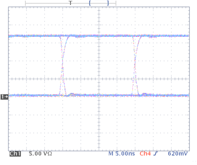
GUID-0494607F-A5BB-4519-8DCD-52CB3A35C672-low.pngFigure 10-5 Typical Driver Output Eye Pattern in Point-to-Point System