ZHCSNB1 February   2021 INA183

PRODUCTION DATA  

  1. 特性
  2. 应用
  3. 说明
  4. Revision History
  5. Device Comparison
  6. Pin Configuration and Functions
  7. Specifications
    1. 7.1 Absolute Maximum Ratings
    2. 7.2 ESD Ratings
    3. 7.3 Recommended Operating Conditions
    4. 7.4 Thermal Information
    5. 7.5 Electrical Characteristics
    6. 7.6 Typical Characteristics
  8. Detailed Description
    1. 8.1 Overview
    2. 8.2 Functional Block Diagram
    3. 8.3 Feature Description
      1. 8.3.1 Single-Supply Operation from IN+
      2. 8.3.2 Low Gain Error and Offset Voltage
      3. 8.3.3 Low Drift Architecture
    4. 8.4 Device Functional Modes
      1. 8.4.1 Normal Operation
      2. 8.4.2 Unidirectional, High-Side Operation
      3. 8.4.3 Input Differential Overload
  9. Application and Implementation
    1. 9.1 Application Information
      1. 9.1.1 RSENSE and Device Gain Selection
    2. 9.2 Typical Application
      1. 9.2.1 Design Requirements
      2. 9.2.2 Detailed Design Procedure
      3. 9.2.3 Application Curve
  10. 10Power Supply Recommendations
  11. 11Layout
    1. 11.1 Layout Guidelines
    2. 11.2 Layout Example
  12. 12Device and Documentation Support
    1. 12.1 Documentation Support
      1. 12.1.1 Related Documentation
    2. 12.2 接收文档更新通知
    3. 12.3 支持资源
    4. 12.4 Trademarks
    5. 12.5 静电放电警告
    6. 12.6 术语表
  13. 13Mechanical, Packaging, and Orderable Information

Pin Configuration and Functions

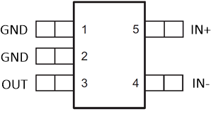
GUID-4AF163B0-3E88-4FC3-82C3-DFAF2DDADB57-low.gifFigure 6-1 DBV Package5-Pin SOT-23Top View
Table 6-1 Pin Functions
PIN I/O DESCRIPTION
NAME SOT-23
GND 1, 2 Analog Device ground. Both pins must be connected to ground.
IN– 4 Analog input Connect to load side of shunt resistor.
IN+ 5 Analog input Connect to supply side of shunt resistor.
OUT 3 Analog output Output voltage.