ZHCSNG6 November 2021 UCC28781-Q1
PRODUCTION DATA
- 1 特性
- 2 应用
- 3 说明
- 4 Revision History
- 5 Pin Configuration and Functions
- 6 Specifications
-
7 Detailed Description
- 7.1 Overview
- 7.2 Functional Block Diagram
- 7.3
Detailed Pin Description
- 7.3.1 BUR Pin (Programmable Burst Mode)
- 7.3.2 FB Pin (Feedback Pin)
- 7.3.3 REF Pin (Internal 5-V Bias)
- 7.3.4 VDD Pin (Device Bias Supply)
- 7.3.5 P13 and SWS Pins
- 7.3.6 S13 Pin
- 7.3.7 IPC Pin (Intelligent Power Control Pin)
- 7.3.8 RUN Pin (Driver and Bias Source for Isolator)
- 7.3.9 PWMH and AGND Pins
- 7.3.10 PWML and PGND Pins
- 7.3.11 SET Pin
- 7.3.12 RTZ Pin (Sets Delay for Transition Time to Zero)
- 7.3.13 RDM Pin (Sets Synthesized Demagnetization Time for ZVS Tuning)
- 7.3.14 XCD Pin
- 7.3.15 CS, VS, and FLT Pins
- 7.4
Device Functional Modes
- 7.4.1 Adaptive ZVS Control with Auto-Tuning
- 7.4.2 Dead-Time Optimization
- 7.4.3 EMI Dither and Dither Fading Function
- 7.4.4 Control Law Across Entire Load Range
- 7.4.5 Adaptive Amplitude Modulation (AAM)
- 7.4.6 Adaptive Burst Mode (ABM)
- 7.4.7 Low Power Mode (LPM)
- 7.4.8 First Standby Power Mode (SBP1)
- 7.4.9 Second Standby Power Mode (SBP2)
- 7.4.10 Startup Sequence
- 7.4.11 Survival Mode of VDD (INT_STOP)
- 7.4.12
System Fault Protections
- 7.4.12.1 Brown-In and Brown-Out
- 7.4.12.2 Output Over-Voltage Protection (OVP)
- 7.4.12.3 Input Over Voltage Protection (IOVP)
- 7.4.12.4 Over-Temperature Protection (OTP) on FLT Pin
- 7.4.12.5 Over-Temperature Protection (OTP) on CS Pin
- 7.4.12.6 Programmable Over-Power Protection (OPP)
- 7.4.12.7 Peak Power Limit (PPL)
- 7.4.12.8 Output Short-Circuit Protection (SCP)
- 7.4.12.9 Over-Current Protection (OCP)
- 7.4.12.10 External Shutdown
- 7.4.12.11 Internal Thermal Shutdown
- 7.4.13 Pin Open/Short Protections
-
8 Application and Implementation
- 8.1 Application Information
- 8.2
Typical Application Circuit
- 8.2.1 Design Requirements for a 60-W, 15-V ZVSF Bias Supply Application with a DC Input
- 8.2.2 Detailed Design Procedure
- 8.2.3 Application Curves
- 9 Power Supply Recommendations
- 10Layout
- 11Device and Documentation Support
- 12Mechanical, Packaging, and Orderable Information
7.4.12.4 Over-Temperature Protection (OTP) on FLT Pin
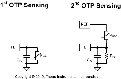
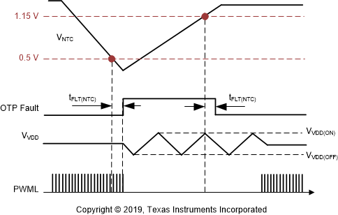
The UCC28781-Q1 uses an external NTC resistor (RNTC) tied to the FLT pin to program a thermal shutdown temperature near the hotspot of the converter. The NTC shutdown threshold (VNTCTH) of 0.5 V with an internal 50-μA current source flowing through RNTC results in a 10-kΩ thermistor shutdown threshold. If the NTC resistance stays lower than 10 kΩ for more than 50 μs, an OTP fault event is triggered. The 50-μs delay (tFLT(NTC)) allows a filter capacitor (CFLT) to be placed between the FLT pin and the AGND pin, when the NTC resistor is located far away from the controller but close to the hot spot. To avoid the OTP fault from false trigger as RUN goes high, CFLT should be designed to allow VFLT increased above VNTCTH within tFLT(NTC). On the other hand, if the NTC resistor is close to the controller and there is no potential noise coupling path to the sensing traces, CFLT is not needed.
For auto-recovery mode, the 0.5-V threshold is increased to 1.15 V after the OTP fault, so the NTC resistance has to increase above 23 kΩ to reset the OTP fault. This threshold change provides a safe temperature hysteresis to help the hot-spot temperature cool down before the next VO restart attempt, reducing the thermal stress to the components. If the FLT pin is not used, the pin can be left floating but can not be connected to REF pin, since the line OVP will be falsely triggered.
The thermal issue in the heavy output load condition is the main design consideration for OTP, and the heavy load operating mode, AAM, allows the controller to stay in the run state continuously, so the 50-μs delay allows VFLT to trigger OTP. Based on the practical BUR-pin setting, 50% to 60% load is operated in AAM. The 50-μA current source is disabled in the burst off time of the light load modes such as ABM, LPM, SBP1, and SBP2, in order to save standby power. However, when the run state becomes shorter than the 50-μs in these modes but the current source is disabled in the wait state, the OTP will not be able to trigger because there is not enough time to detect the fault. Therefore, if certain design considerations still require the OTP to be armed in light load modes, a second OTP configuration can be considered by reusing the 4.5-V threshold of input OVP. As shown in Figure 7-40, the upper NTC resistor and the lower resistor form a resistor divider from the REF pin to the FLT pin. The 750-μs delay is independent to the wait state condition of controller, so the OTP fault can still be triggered in the light load mode. This configuration provides auto-recovery mode only.
 Figure 7-40 Two Connections to Implement OTP on the FLT Pin
 Figure 7-41 OTP Timing Diagram for a NTC between the FLT Pin and AGND Pin