ZHCSNG6 November 2021 UCC28781-Q1
PRODUCTION DATA
- 1 特性
- 2 应用
- 3 说明
- 4 Revision History
- 5 Pin Configuration and Functions
- 6 Specifications
-
7 Detailed Description
- 7.1 Overview
- 7.2 Functional Block Diagram
- 7.3
Detailed Pin Description
- 7.3.1 BUR Pin (Programmable Burst Mode)
- 7.3.2 FB Pin (Feedback Pin)
- 7.3.3 REF Pin (Internal 5-V Bias)
- 7.3.4 VDD Pin (Device Bias Supply)
- 7.3.5 P13 and SWS Pins
- 7.3.6 S13 Pin
- 7.3.7 IPC Pin (Intelligent Power Control Pin)
- 7.3.8 RUN Pin (Driver and Bias Source for Isolator)
- 7.3.9 PWMH and AGND Pins
- 7.3.10 PWML and PGND Pins
- 7.3.11 SET Pin
- 7.3.12 RTZ Pin (Sets Delay for Transition Time to Zero)
- 7.3.13 RDM Pin (Sets Synthesized Demagnetization Time for ZVS Tuning)
- 7.3.14 XCD Pin
- 7.3.15 CS, VS, and FLT Pins
- 7.4
Device Functional Modes
- 7.4.1 Adaptive ZVS Control with Auto-Tuning
- 7.4.2 Dead-Time Optimization
- 7.4.3 EMI Dither and Dither Fading Function
- 7.4.4 Control Law Across Entire Load Range
- 7.4.5 Adaptive Amplitude Modulation (AAM)
- 7.4.6 Adaptive Burst Mode (ABM)
- 7.4.7 Low Power Mode (LPM)
- 7.4.8 First Standby Power Mode (SBP1)
- 7.4.9 Second Standby Power Mode (SBP2)
- 7.4.10 Startup Sequence
- 7.4.11 Survival Mode of VDD (INT_STOP)
- 7.4.12
System Fault Protections
- 7.4.12.1 Brown-In and Brown-Out
- 7.4.12.2 Output Over-Voltage Protection (OVP)
- 7.4.12.3 Input Over Voltage Protection (IOVP)
- 7.4.12.4 Over-Temperature Protection (OTP) on FLT Pin
- 7.4.12.5 Over-Temperature Protection (OTP) on CS Pin
- 7.4.12.6 Programmable Over-Power Protection (OPP)
- 7.4.12.7 Peak Power Limit (PPL)
- 7.4.12.8 Output Short-Circuit Protection (SCP)
- 7.4.12.9 Over-Current Protection (OCP)
- 7.4.12.10 External Shutdown
- 7.4.12.11 Internal Thermal Shutdown
- 7.4.13 Pin Open/Short Protections
-
8 Application and Implementation
- 8.1 Application Information
- 8.2
Typical Application Circuit
- 8.2.1 Design Requirements for a 60-W, 15-V ZVSF Bias Supply Application with a DC Input
- 8.2.2 Detailed Design Procedure
- 8.2.3 Application Curves
- 9 Power Supply Recommendations
- 10Layout
- 11Device and Documentation Support
- 12Mechanical, Packaging, and Orderable Information
7.3.14 XCD Pin
The XCD pin performs the X-capacitor discharge function in conjunction with the recommended external detection circuit, shown in Figure 7-17.
If the XCD function is not needed, directly shorting the two XCD pins to the AGND pin disables the XCD pin function, so the controller wait-state current is further reduced. The external sensing circuit must be removed. (see Figure 7-18)
To form the discharge path in the first circuit, the anode nodes of two high-voltage diode rectifiers are connected to each X-cap terminal, the two diode cathodes are connected together to a 26-kΩ current limit resistance (RXCD), and the drain-to-source of a high-voltage depletion MOSFET (QXCD) couples the resistance to XCD pins. Since RXCD needs to sustain the high voltage drop from the XCD-pin current, two series 13-kΩ SMD resistors in 1206 size with 26-kΩ total resistance are required to meet the voltage de-rating. A 600-V rated MOSFET such as BSS126 is needed as the high voltage blocking device. The MOSFET gate is connected to the P13 pin, so the highest voltage level of the XCD pins is limited to the sum of the P13-pin voltage and the threshold voltage of BSS126. The voltage level gives sufficient headroom over the 6.5-V line zero-crossing (LZC) threshold.
In case of single-fault event where one XCD pin is in fail-open condition, the redundant XCD pin helps to maintain the X-cap discharge function. In case of the single-fault event of BSS126 involving its drain-to-source in fail-short condition, an internal 26-V clamp helps to protect the XCD pin from exceeding its voltage rating. The current-limiting resistance (RXCD) limits the fault current below the maximum clamping capability, however the value of RXCD should avoid reducing the normal discharge current. A total resistance of 26 kΩ ±5% meets both criteria. The internal clamping function can also help to dissipate some of the line surge energy accumulated on the XCD pins in order to limit the pin voltage below its 30-V rating.
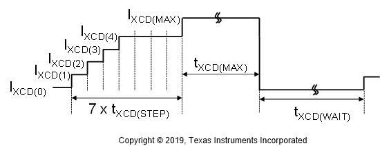
After the AC line is disconnected, X-capacitors in the EMI filters on the AC side of the diode-bridge rectifier must have means to discharge its residual voltage to a safe level within a certain time. Typically a high voltage discharge resistor bank is placed in parallel with the capacitor to form a discharge path. The value of the resistance is chosen to discharge the capacitance within the required time period. However, if the capacitance is large enough, the necessary lower value of discharge resistance will increase the standby power. The controller provides an active X-capacitor discharge function with 2-mA maximum discharge current capability to reduce the standby power. The discharge current is activated only when the detection criteria for the AC-line removal condition is met. The 6.5-V line zero-crossing (LZC) threshold on XCD pins is used to detect AC-line presence. When LZC is missing over an 84-ms detection timeout period, the discharge current is enabled for a maximum period of 300 ms followed by a 700-ms blanking time with no current. To detect the zero crossing reliably, as well as to save power consumption, a stair-case test current shown in Figure 7-19 is generated within the 84-ms detection time. The worst-case discharge current and timing are designed to discharge the X-capacitor up to 1 µF.
 Figure 7-19 Step-current Profile into the XCD Pins for the X-cap Discharge Function
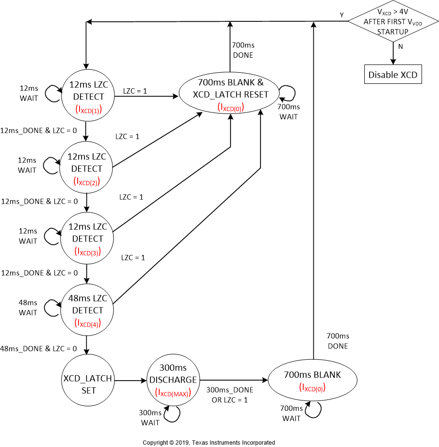
The four test current levels are designed to overcome the impact of leakage current from the bridge diode over a wide line range. Without enough test current level in a 12-ms period, the diode leakage current will prevent the XCD-pin voltage from reaching close to the 6.5-V LZC threshold. A higher AC line voltage or a higher diode junction temperature requires a higher test current due to the increased diode leakage current. When the AC line is connected, the four stair-case current levels and the 700-ms time out after the completion of LZC detection helps to minimize the average current sink from AC main and thereby the static power loss. For the first three current levels, every 12-ms time-out event commands the test current to increment. The last test current level has to be sustained for 48 ms without LZC, before triggering the 2-mA discharge mode. Whenever LZC is detected, any higher-level test-current steps are aborted and the 700-ms wait-state is initiated. Figure 7-20 shows the flow chart of X-capacitor discharge.
Note that the XCD-LATCH referenced in Figure 7-20 is a latch that is set when loss of AC line is confirmed. When set, this state allows X-capacitor discharge to proceed.
 Figure 7-20 The State Diagram of the XCD-pin Function
Whenever any system protection is triggered, the converter switching is terminated and VVDD restart cycle occurs between VVDD(ON) and VVDD(OFF). In this mode, the XCD pin function continues to operate, since the internal circuitry is separately biased from VVDD instead of from VREF.
Shorting the XCD pins to AGND disables the XCD function. After VVDD first reaches VVDD(ON), an 80-µA test current is sourced out of the XCD pin in order to reliably identify the XCD-pin short with a low-impedance path to the AGND pin. If XCD is shorted to AGND, any path to L and N must be open to prevent RXCD from overheating. When VXCD is lower than 4 V before the RUN-pin first pulls high, the XCD function is disabled and the internal circuit will stop sourcing current from VVDD.