ZHCSNG6 November 2021 UCC28781-Q1
PRODUCTION DATA
- 1 特性
- 2 应用
- 3 说明
- 4 Revision History
- 5 Pin Configuration and Functions
- 6 Specifications
-
7 Detailed Description
- 7.1 Overview
- 7.2 Functional Block Diagram
- 7.3
Detailed Pin Description
- 7.3.1 BUR Pin (Programmable Burst Mode)
- 7.3.2 FB Pin (Feedback Pin)
- 7.3.3 REF Pin (Internal 5-V Bias)
- 7.3.4 VDD Pin (Device Bias Supply)
- 7.3.5 P13 and SWS Pins
- 7.3.6 S13 Pin
- 7.3.7 IPC Pin (Intelligent Power Control Pin)
- 7.3.8 RUN Pin (Driver and Bias Source for Isolator)
- 7.3.9 PWMH and AGND Pins
- 7.3.10 PWML and PGND Pins
- 7.3.11 SET Pin
- 7.3.12 RTZ Pin (Sets Delay for Transition Time to Zero)
- 7.3.13 RDM Pin (Sets Synthesized Demagnetization Time for ZVS Tuning)
- 7.3.14 XCD Pin
- 7.3.15 CS, VS, and FLT Pins
- 7.4
Device Functional Modes
- 7.4.1 Adaptive ZVS Control with Auto-Tuning
- 7.4.2 Dead-Time Optimization
- 7.4.3 EMI Dither and Dither Fading Function
- 7.4.4 Control Law Across Entire Load Range
- 7.4.5 Adaptive Amplitude Modulation (AAM)
- 7.4.6 Adaptive Burst Mode (ABM)
- 7.4.7 Low Power Mode (LPM)
- 7.4.8 First Standby Power Mode (SBP1)
- 7.4.9 Second Standby Power Mode (SBP2)
- 7.4.10 Startup Sequence
- 7.4.11 Survival Mode of VDD (INT_STOP)
- 7.4.12
System Fault Protections
- 7.4.12.1 Brown-In and Brown-Out
- 7.4.12.2 Output Over-Voltage Protection (OVP)
- 7.4.12.3 Input Over Voltage Protection (IOVP)
- 7.4.12.4 Over-Temperature Protection (OTP) on FLT Pin
- 7.4.12.5 Over-Temperature Protection (OTP) on CS Pin
- 7.4.12.6 Programmable Over-Power Protection (OPP)
- 7.4.12.7 Peak Power Limit (PPL)
- 7.4.12.8 Output Short-Circuit Protection (SCP)
- 7.4.12.9 Over-Current Protection (OCP)
- 7.4.12.10 External Shutdown
- 7.4.12.11 Internal Thermal Shutdown
- 7.4.13 Pin Open/Short Protections
-
8 Application and Implementation
- 8.1 Application Information
- 8.2
Typical Application Circuit
- 8.2.1 Design Requirements for a 60-W, 15-V ZVSF Bias Supply Application with a DC Input
- 8.2.2 Detailed Design Procedure
- 8.2.3 Application Curves
- 9 Power Supply Recommendations
- 10Layout
- 11Device and Documentation Support
- 12Mechanical, Packaging, and Orderable Information
7.4.2 Dead-Time Optimization
The dead-time optimizer in Figure 7-21 controls the two dead-times: the dead-time between PWMH falling edge and PWML rising edge (tZ), as well as the dead-time between PWML falling edge and PWMH rising edge (tD(PWML-H)).
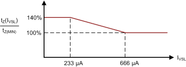
The adaptive control law for tZ utilizes the line feed-forward signal to extend tZ as VBULK reduces, as shown in Figure 7-23. The VS pin senses VBULK through the auxiliary winding voltage (VAUX) when the primary side switch (QL) is on. The auxiliary winding creates a line-sensing current (IVSL) out of the VS pin flowing through the upper resistor of the voltage divider on VS pin (RVS1). Minimum tZ (tZ(MIN)) is set at VBULK(MAX) through the RTZ pin. When IVSL is lower than 666 μA, tZ linearly increases and the maximum tZ extension is 140% of tZ(MIN).
 Figure 7-23 tZ Control Optimized for Wide Input Voltage Range
The control law for tD(PWML-H) is adaptive with the slope variation of the switching node voltage, regardless of the SET-pin voltage as shown in Figure 7-24.