ZHCSNG6 November 2021 UCC28781-Q1
PRODUCTION DATA
- 1 特性
- 2 应用
- 3 说明
- 4 Revision History
- 5 Pin Configuration and Functions
- 6 Specifications
-
7 Detailed Description
- 7.1 Overview
- 7.2 Functional Block Diagram
- 7.3
Detailed Pin Description
- 7.3.1 BUR Pin (Programmable Burst Mode)
- 7.3.2 FB Pin (Feedback Pin)
- 7.3.3 REF Pin (Internal 5-V Bias)
- 7.3.4 VDD Pin (Device Bias Supply)
- 7.3.5 P13 and SWS Pins
- 7.3.6 S13 Pin
- 7.3.7 IPC Pin (Intelligent Power Control Pin)
- 7.3.8 RUN Pin (Driver and Bias Source for Isolator)
- 7.3.9 PWMH and AGND Pins
- 7.3.10 PWML and PGND Pins
- 7.3.11 SET Pin
- 7.3.12 RTZ Pin (Sets Delay for Transition Time to Zero)
- 7.3.13 RDM Pin (Sets Synthesized Demagnetization Time for ZVS Tuning)
- 7.3.14 XCD Pin
- 7.3.15 CS, VS, and FLT Pins
- 7.4
Device Functional Modes
- 7.4.1 Adaptive ZVS Control with Auto-Tuning
- 7.4.2 Dead-Time Optimization
- 7.4.3 EMI Dither and Dither Fading Function
- 7.4.4 Control Law Across Entire Load Range
- 7.4.5 Adaptive Amplitude Modulation (AAM)
- 7.4.6 Adaptive Burst Mode (ABM)
- 7.4.7 Low Power Mode (LPM)
- 7.4.8 First Standby Power Mode (SBP1)
- 7.4.9 Second Standby Power Mode (SBP2)
- 7.4.10 Startup Sequence
- 7.4.11 Survival Mode of VDD (INT_STOP)
- 7.4.12
System Fault Protections
- 7.4.12.1 Brown-In and Brown-Out
- 7.4.12.2 Output Over-Voltage Protection (OVP)
- 7.4.12.3 Input Over Voltage Protection (IOVP)
- 7.4.12.4 Over-Temperature Protection (OTP) on FLT Pin
- 7.4.12.5 Over-Temperature Protection (OTP) on CS Pin
- 7.4.12.6 Programmable Over-Power Protection (OPP)
- 7.4.12.7 Peak Power Limit (PPL)
- 7.4.12.8 Output Short-Circuit Protection (SCP)
- 7.4.12.9 Over-Current Protection (OCP)
- 7.4.12.10 External Shutdown
- 7.4.12.11 Internal Thermal Shutdown
- 7.4.13 Pin Open/Short Protections
-
8 Application and Implementation
- 8.1 Application Information
- 8.2
Typical Application Circuit
- 8.2.1 Design Requirements for a 60-W, 15-V ZVSF Bias Supply Application with a DC Input
- 8.2.2 Detailed Design Procedure
- 8.2.3 Application Curves
- 9 Power Supply Recommendations
- 10Layout
- 11Device and Documentation Support
- 12Mechanical, Packaging, and Orderable Information
7.4.12.3 Input Over Voltage Protection (IOVP)
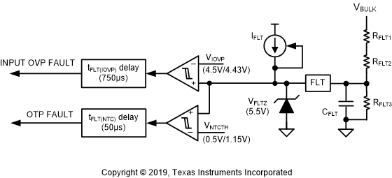
The UCC28781-Q1 provides an input OVP function on the FLT pin. Figure 7-39 shows the application circuit for the input OVP sensing. A resistor divider senses the bulk capacitor voltage, and the IOVP fault is triggered when VFLT > 4.5 V for longer than 750 µs. The 750 µs delay helps to desensitize the abrupt bulk voltage spike during the line surge condition, such that the output voltage will not drop accidentally. After the IOVP fault is asserted, the switching will be terminated immediately and VVDD will restart. When VVDD reaches VVDD(ON) of the following VDD cycle, the controller will check VFLT first before switching, to avoid the switching device from being exposed to a high-voltage stress condition. The fault will be cleared when VFLT < 4.43 V.
If longer than 750 µs delay is required, a filter capacitor between the FLT pin and AGND pin can create additional programmable delay. If the filter capacitor is too large, it may trigger the OTP fault on the FLT pin, if the ramp up time for VFLT to rise above VNTCTH is longer than tFLT(NTC) after the RUN pin is pulled high. The resistor divider design does not need to consider the offset voltage effect from the 50 µA current source out of the FLT pin, because the controller will disable the current source once VFLT > 2.5 V.
The goal of the internal 5.5-V clamp device on the FLT pin is to protect the pin from exceeding the voltage limit when one of the IOVP upper sensing resistor fails short. The maximum clamp current is 150 µA, so the resistor divider design needs to consider this limitation.
 Figure 7-39 Bulk Capacitor Voltage Sensing for Input OVP