ZHCSNG6 November 2021 UCC28781-Q1
PRODUCTION DATA
- 1 特性
- 2 应用
- 3 说明
- 4 Revision History
- 5 Pin Configuration and Functions
- 6 Specifications
-
7 Detailed Description
- 7.1 Overview
- 7.2 Functional Block Diagram
- 7.3
Detailed Pin Description
- 7.3.1 BUR Pin (Programmable Burst Mode)
- 7.3.2 FB Pin (Feedback Pin)
- 7.3.3 REF Pin (Internal 5-V Bias)
- 7.3.4 VDD Pin (Device Bias Supply)
- 7.3.5 P13 and SWS Pins
- 7.3.6 S13 Pin
- 7.3.7 IPC Pin (Intelligent Power Control Pin)
- 7.3.8 RUN Pin (Driver and Bias Source for Isolator)
- 7.3.9 PWMH and AGND Pins
- 7.3.10 PWML and PGND Pins
- 7.3.11 SET Pin
- 7.3.12 RTZ Pin (Sets Delay for Transition Time to Zero)
- 7.3.13 RDM Pin (Sets Synthesized Demagnetization Time for ZVS Tuning)
- 7.3.14 XCD Pin
- 7.3.15 CS, VS, and FLT Pins
- 7.4
Device Functional Modes
- 7.4.1 Adaptive ZVS Control with Auto-Tuning
- 7.4.2 Dead-Time Optimization
- 7.4.3 EMI Dither and Dither Fading Function
- 7.4.4 Control Law Across Entire Load Range
- 7.4.5 Adaptive Amplitude Modulation (AAM)
- 7.4.6 Adaptive Burst Mode (ABM)
- 7.4.7 Low Power Mode (LPM)
- 7.4.8 First Standby Power Mode (SBP1)
- 7.4.9 Second Standby Power Mode (SBP2)
- 7.4.10 Startup Sequence
- 7.4.11 Survival Mode of VDD (INT_STOP)
- 7.4.12
System Fault Protections
- 7.4.12.1 Brown-In and Brown-Out
- 7.4.12.2 Output Over-Voltage Protection (OVP)
- 7.4.12.3 Input Over Voltage Protection (IOVP)
- 7.4.12.4 Over-Temperature Protection (OTP) on FLT Pin
- 7.4.12.5 Over-Temperature Protection (OTP) on CS Pin
- 7.4.12.6 Programmable Over-Power Protection (OPP)
- 7.4.12.7 Peak Power Limit (PPL)
- 7.4.12.8 Output Short-Circuit Protection (SCP)
- 7.4.12.9 Over-Current Protection (OCP)
- 7.4.12.10 External Shutdown
- 7.4.12.11 Internal Thermal Shutdown
- 7.4.13 Pin Open/Short Protections
-
8 Application and Implementation
- 8.1 Application Information
- 8.2
Typical Application Circuit
- 8.2.1 Design Requirements for a 60-W, 15-V ZVSF Bias Supply Application with a DC Input
- 8.2.2 Detailed Design Procedure
- 8.2.3 Application Curves
- 9 Power Supply Recommendations
- 10Layout
- 11Device and Documentation Support
- 12Mechanical, Packaging, and Orderable Information
7.3.2 FB Pin (Feedback Pin)
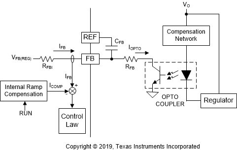
The FB pin usually connects to the collector of an optocoupler output transistor through an external current-limiting resistor (RFB). A maximum of 20 kΩ for RFB is recommended. The feedback network of UCC28781-Q1 is shown in Figure 7-3. A high-quality ceramic by-pass capacitor between FB pin and REF pin (CFB) is required for decoupling IFB from switching noise interference. A minimum of 220 pF is recommended for CFB . An internal 8-kΩ resistor (RFBI) at the FB pin in conjunction with the external CFB forms an effective low-pass filter. Section 8 provides a detailed design guide on the secondary-side compensation network of VO feedback loop, to improve the load transient response and also limit the IFB ripple of ABM mode within the recommended range.
 Figure 7-3 External Feedback Network Connected to the FB Pin
Depending on the operating mode, the controller interprets the current flowing out of the FB pin (IFB) to regulate the output voltage. For AAM and LPM modes based on peak current control, IFB is converted into an internal peak current-sense threshold (VCST) to modulate the amplitude of the current-sense signal on the CS pin. For example, when the output voltage (VO) is lower than the regulation level set by the shunt regulator, the absolute current level of IFB reduces, causing a higher VCST to increase more power to the output load. In ABM, the burst control loop takes over the VO regulation, where VCST is clamped to VCST(BUR) and the ripple component of IFB participates in the modulation of the burst off time.
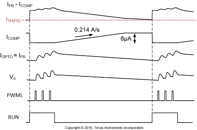
Figure 7-4 illustrates the operating principle of the ABM. A burst of switching pulses raises the output voltage VO which increases IFB. At the end of the burst, the load current discharges the output capacitor, which decreases VO and IFB. UCC28781-Q1 injects a noise-free internal ramp compensation current (ICOMP) superimposed on IFB in order to stabilize the ABM operation. When the RUN pin is high, ICOMP is reset to 0 μA. When the RUN pin goes low, ICOMP is gradually increased to 6 μA with a positive slope of 0.214 A/s. The summation of IFB and ICOMP is compared with ITH(FB) to trigger the next burst event. The magnitude and sharp slope of ICOMP help to push switching ripple and high-frequency noise component of IOPTO away from ITH(FB).
 Figure 7-4 Concept of Burst Control with an Internal Ramp Compensation