ZHCSNI0B March 2021 – November 2022 TMUX7411F , TMUX7412F , TMUX7413F
PRODMIX
- 1 特性
- 2 应用
- 3 说明
- 4 Revision History
- 5 Device Comparison Table
- 6 Pin Configuration and Functions
-
7 Specifications
- 7.1 Absolute Maximum Ratings
- 7.2 ESD Ratings
- 7.3 Thermal Information
- 7.4 Recommended Operating Conditions
- 7.5 Electrical Characteristics: Global
- 7.6 ±15 V Dual Supply: Electrical Characteristics
- 7.7 ±20 V Dual Supply: Electrical Characteristics
- 7.8 12 V Single Supply: Electrical Characteristics
- 7.9 36 V Single Supply: Electrical Characteristics
- 7.10 Typical Characteristics
-
8 Parameter Measurement Information
- 8.1 On-Resistance
- 8.2 Turn-On and Turn-Off Time
- 8.3 Off-Leakage Current
- 8.4 On-Leakage Current
- 8.5 Input and Output Leakage Current Under Overvoltage Fault
- 8.6 Fault Response Time
- 8.7 Fault Recovery Time
- 8.8 Fault Flag Response Time
- 8.9 Fault Flag Recovery Time
- 8.10 Charge Injection
- 8.11 Off Isolation
- 8.12 Inter-Channel Crosstalk
- 8.13 Bandwidth
- 8.14 THD + Noise
- 9 Detailed Description
- 10Application and Implementation
- 11Power Supply Recommendations
- 12Layout
- 13Device and Documentation Support
- 14Mechanical, Packaging, and Orderable Information
8.4 On-Leakage Current
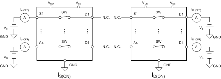
Source on-leakage current (IS(ON)) and drain on-leakage current (ID(ON)) denote the channel leakage currents when the switch is in the on state. IS(ON) is measured with the drain floating, while ID(ON) is measured with the source floating. Figure 8-4 shows the circuit used for measuring the on-leakage currents.
 Figure 8-4 On-Leakage Measurement Setup