ZHCSNM5C november 2020 – august 2023 UCC25800-Q1
PRODUCTION DATA
- 1
- 1 特性
- 2 应用
- 3 说明
- 4 Revision History
- 5 Device Comparison Table
- 6 Pin Configuration and Functions
- 7 Specifications
- 8 Detailed Description
- 9 Application and Implementation
- 10Power Supply Recommendations
- 11Layout
- 12Device and Documentation Support
- 13Mechanical, Packaging, and Orderable Information
8.3.2 Oscillator
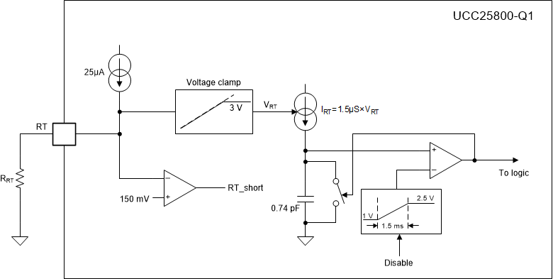
The internal oscillator of the UCC25800-Q1 transformer driver sets the switching frequency of the power stage. It operates at a 50% duty cycle. The voltage on the RT pin sets the oscilator frequency. A 25-µA current source flows out of the pin so that the switching frequency can be set by connecting a resistor to GND. Figure 8-1 shows the internal oscillator.
 Figure 8-1 Equivalent circuit for internal
oscillator
Figure 8-1 Equivalent circuit for internal
oscillatorUse Equation 1 to calculate the RT pin resitance for a required switching frequency.
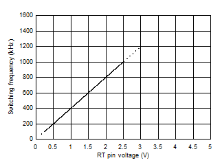
If the RT pin is left open, or an RT pin resistor value results in an RT pin voltage at RTOPEN threshold or above, the power stage operates with the default switching frequency of 1.2 MHz. If the RT pin voltage is below 150 mV, the transformer driver considers the RT pin shorted to ground and declares a fault. The programmable voltage range on the RT pin is 250 mV to 2.5 V. The relationship between the power stage switching frequency and the RT-pin voltage is shown in Figure 8-2.
 Figure 8-2 Relationship between switching
frequency and RT-pin voltage
Figure 8-2 Relationship between switching
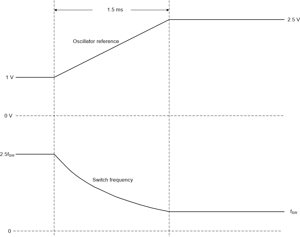
frequency and RT-pin voltageTo avoid the excessive current stress during the start-up process, the transformer driver integrates a soft-start function. The oscillator starts by ramping the oscillator reference from 1 V to 2.5 V, which results in the switching frequency reducing from 2.5 times of the set frequency to the set frequency. Because the current source in the oscillator remains the same while the reference changes, the switching cycle decays linearly. The soft-start time is fixed internally at 1.5 ms. This long soft-start time limits the inrush current when charging large output capacitors. The soft-start is enabled during the start-up and fault recovery process. Figure 8-3 shows the switching frequency variation during the start-up time.
 Figure 8-3 Switching frequency during soft start
time
Figure 8-3 Switching frequency during soft start
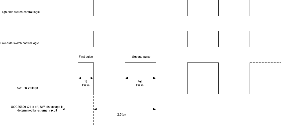
timeDuring the soft-start sequence, the first pulse from the oscillator is a half of the second pulse width (25% of the period at the starting switching frequency) and followed immediately by 50% duty cycle pulses. This process ensures the LLC transformer magnetizing current is symmetrical from the first pulse to minimize ringing in the system. The high-side switch is always turned on at the first pulse to avoid uncertainty of the circuit operation.
 Figure 8-4 SW pin voltage and control logic at
the first switching cycle (dead-time is not shown)