ZHCSNM5C november   2020  – august 2023 UCC25800-Q1

PRODUCTION DATA  

  1.   1
  2. 特性
  3. 应用
  4. 说明
  5. Revision History
  6. Device Comparison Table
  7. Pin Configuration and Functions
  8. Specifications
    1. 7.1 Absolute Maximum Ratings
    2. 7.2 ESD Ratings
    3. 7.3 Recommended Operating Conditions
    4. 7.4 Thermal Information
    5. 7.5 Electrical Characteristics
    6. 7.6 Typical Characteristics
  9. Detailed Description
    1. 8.1 Overview
    2. 8.2 Functional Block Diagram
    3. 8.3 Feature Description
      1. 8.3.1 Power Management
      2. 8.3.2 Oscillator
      3. 8.3.3 External Synchronization
      4. 8.3.4 Dead-Time
        1. 8.3.4.1 Adaptive Dead-time
        2. 8.3.4.2 Maximum Programmable Dead-time
      5. 8.3.5 Protections
        1. 8.3.5.1 Overcurrent Protection
          1. 8.3.5.1.1 OCP Threshold Setting
          2. 8.3.5.1.2 Output Power Capability
        2. 8.3.5.2 Input Overvoltage Protection (OVP)
        3. 8.3.5.3 Over-Temperature Protection (TSD)
        4. 8.3.5.4 Pin-Fault Protections
        5. 8.3.5.5 VREG Pin Protection
      6. 8.3.6 DIS/FLT Pin operation
        1. 8.3.6.1 FAULT Codes
    4. 8.4 Device Functional Modes
      1. 8.4.1 UVLO Mode
      2. 8.4.2 Soft-start Mode
      3. 8.4.3 Normal Operation Mode
      4. 8.4.4 Disabled Mode
      5. 8.4.5 Fault Modes
  10. Application and Implementation
    1. 9.1 Application Information
    2. 9.2 Typical Application
      1. 9.2.1 LLC Converter Operation Principle
      2. 9.2.2 Design Requirements
      3. 9.2.3 Detailed Design Procedure
      4. 9.2.4 Application Curves
    3. 9.3 What to Do and What Not to Do
  11. 10Power Supply Recommendations
  12. 11Layout
    1. 11.1 Layout Guidelines
    2. 11.2 Layout Example
  13. 12Device and Documentation Support
    1. 12.1 Documentation Support
      1. 12.1.1 Related Documentation
    2. 12.2 接收文档更新通知
    3. 12.3 支持资源
    4. 12.4 Trademarks
    5. 12.5 静电放电警告
    6. 12.6 术语表
  14. 13Mechanical, Packaging, and Orderable Information

FAULT Codes

When the UCC25800-Q1 transformer driver enters fault mode, it outputs a train of pulses to indicate which faults have occurred through the DIS/FLT pin. The pulse train consists of a number 50% duty cycle pulses at 50 kHz, (that is, 10-μs wide pulses), where the number of pulses indicates the fault listed in Table 8-4. The pulse train is created through controlling the internal 750-μA pull-down current source, together with the 100-kΩ pull-up resistor.

Table 8-4 Fault codes
NO. OF PULSES FAULT
1 OCP1
2 OCP2
3 Input overvoltage protection
4 Over temperature protection
5 DT out of range
6 OC/DT open
7 OC/DT short
8 RT short
9 OTP (one-time-programmable bit ) error

The pulse train starts 10 µs after the fault has been asserted. Transmission of the fault code begins with a 100-µs wide high pulse. If more than one fault is detected, the codes are transmitted successively based on the order in Table 8-4, separated by a 100-μs wide high pulse, as shown below in Figure 8-18.
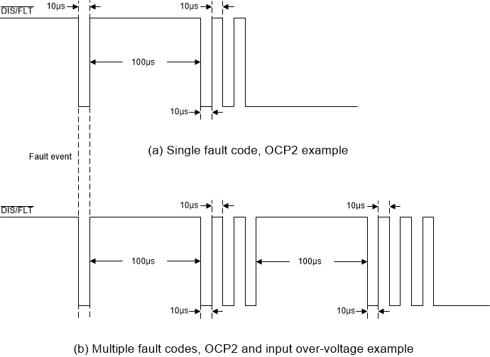
GUID-D379065F-FCBC-4926-8A44-5D6F370C4958-low.gifFigure 8-18 Fault code diagram