ZHCSNY0B May 2020 – January 2023 BQ25798
PRODUCTION DATA
- 1 特性
- 2 应用
- 3 说明
- 4 Revision History
- 5 说明(续)
- 6 Device Comparison
- 7 Pin Configuration and Functions
- 8 Specifications
-
9 Detailed Description
- 9.1 Overview
- 9.2 Functional Block Diagram
- 9.3
Feature Description
- 9.3.1 Device Power-On-Reset
- 9.3.2 PROG Pin Configuration
- 9.3.3 Device Power Up from Battery without Input Source
- 9.3.4 Device Power Up from Input Source
- 9.3.5 Dual-Input Power Mux
- 9.3.6 Buck-Boost Converter Operation
- 9.3.7 USB On-The-Go (OTG)
- 9.3.8 Power Path Management
- 9.3.9 Battery Charging Management
- 9.3.10 Integrated 16-Bit ADC for Monitoring
- 9.3.11 Status Outputs ( STAT, and INT)
- 9.3.12 Ship FET Control
- 9.3.13
Protections
- 9.3.13.1
Voltage and Current Monitoring
- 9.3.13.1.1 VAC Over-voltage Protection (VAC_OVP)
- 9.3.13.1.2 VBUS Over-voltage Protection (VBUS_OVP)
- 9.3.13.1.3 VBUS Under-voltage Protection (POORSRC)
- 9.3.13.1.4 System Over-voltage Protection (VSYS_OVP)
- 9.3.13.1.5 System Short Protection (VSYS_SHORT)
- 9.3.13.1.6 Battery Over-voltage Protection (VBAT_OVP)
- 9.3.13.1.7 Battery Over-current Protection (IBAT_OCP)
- 9.3.13.1.8 Input Over-current Protection (IBUS_OCP)
- 9.3.13.1.9 OTG Over-voltage Protection (OTG_OVP)
- 9.3.13.1.10 OTG Under-voltage Protection (OTG_UVP)
- 9.3.13.2 Thermal Regulation and Thermal Shutdown
- 9.3.13.1
Voltage and Current Monitoring
- 9.3.14 Serial Interface
- 9.4 Device Functional Modes
- 9.5 Register Map
- 10Application and Implementation
- 11Power Supply Recommendations
- 12Layout
- 13Device and Documentation Support
- 14Mechanical, Packaging, and Orderable Information
9.3.12 Ship FET Control
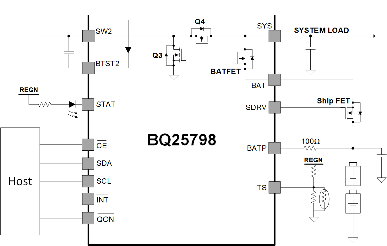
The charger provides an N-FET driving pin (SDRV) to control an external ship FET. The SDRV pin is the output of a charge pump that provides 100 nA typical drive current to drive the ship FET gate to typically 5-V above the battery voltage. When this ship FET is off, it removes leakage current from the battery to the system. The ship FET is controlled by the SDRV_CTRL[1:0] register bits, to support the shutdown mode, ship mode and the system power reset.
- IDLE Mode when SDRV_CTRL[1:0] = 00, POR default. The external ship FET is fully on, I2C is enabled. The internal BATFET status is determined by the charging status. This mode is valid with adapter present, during forward charging, in OTG mode or in the battery only condition.
- Shutdown Mode when SDRV_CTRL[1:0] = 01. The ship FET turns off. The I2C is disabled. The charger is totally shutdown and can only be woken up by an adapter plug-in. This mode can only be entered when no adapter is present. If SDRV_CTRL[1:0] is written to 01 with an adapter present, the write is ignored.
- Ship Mode when SDRV_CTRL[1:0] = 10. The ship FET turns off. The I2C is still enabled. The charger can be woken up by setting SDRV_CTRL[1:0] back to 00, or pulling the QON pin low, or an adapter plug-in. This mode can only be entered when no adapter is present. If SDRV_CTRL[1:0] is written to 01 with an adapter present, the write is ignored.
- System Power Reset when SDRV_CTRL[1:0] = 11. The ship FET is turned off for typical 350ms to reset the system power (converter goes to HIZ mode if VBUS is high), then the ship FET is fully turned on again. The BATFET keeps the status unchanged during the system power reset. After the reset is done, SDRV_CTRL[1:0] goes back to 00.
When the host changes SDRV_CTRL[1:0] from 00 to the other values, the charger turns off the ship FET immediately or delays by tSM_DLY as configured by SDRV_DLY bit. The application diagram when the battery is connected to the charger through an external ship FET is illustrated in the figure below.
 Figure 9-15 The Application Diagram for
the External Ship FET