ZHCSNY0B May   2020  – January 2023 BQ25798

PRODUCTION DATA  

  1. 特性
  2. 应用
  3. 说明
  4. Revision History
  5. 说明(续)
  6. Device Comparison
  7. Pin Configuration and Functions
  8. Specifications
    1. 8.1 Absolute Maximum Ratings
    2. 8.2 ESD Ratings
    3. 8.3 Recommended Operating Conditions
    4. 8.4 Thermal Information
    5. 8.5 Electrical Characteristics
    6. 8.6 Timing Requirements
    7. 8.7 Typical Characteristics
  9. Detailed Description
    1. 9.1 Overview
    2. 9.2 Functional Block Diagram
    3. 9.3 Feature Description
      1. 9.3.1  Device Power-On-Reset
      2. 9.3.2  PROG Pin Configuration
      3. 9.3.3  Device Power Up from Battery without Input Source
      4. 9.3.4  Device Power Up from Input Source
        1. 9.3.4.1 Power Up REGN LDO
        2. 9.3.4.2 Poor Source Qualification
        3. 9.3.4.3 ILIM_HIZ Pin
        4. 9.3.4.4 Default VINDPM Setting
        5. 9.3.4.5 Input Source Type Detection
          1. 9.3.4.5.1 D+/D– Detection Sets Input Current Limit
          2. 9.3.4.5.2 HVDCP Detection Procedure
          3. 9.3.4.5.3 Connector Fault Detection
      5. 9.3.5  Dual-Input Power Mux
        1. 9.3.5.1 ACDRV Turn On Condition
        2. 9.3.5.2 VBUS Input Only
        3. 9.3.5.3 One ACFET-RBFET
        4. 9.3.5.4 Two ACFETs-RBFETs
      6. 9.3.6  Buck-Boost Converter Operation
        1. 9.3.6.1 Force Input Current Limit Detection
        2. 9.3.6.2 Input Current Optimizer (ICO)
        3. 9.3.6.3 Maximum Power Point Tracking for Small PV Panel
        4. 9.3.6.4 Pulse Frequency Modulation (PFM)
        5. 9.3.6.5 Device HIZ State
      7. 9.3.7  USB On-The-Go (OTG)
        1. 9.3.7.1 OTG Mode to Power External Devices
        2. 9.3.7.2 Backup Power Supply Mode
        3. 9.3.7.3 Backup Mode with Dual Input Mux
      8. 9.3.8  Power Path Management
        1. 9.3.8.1 Narrow VDC Architecture
        2. 9.3.8.2 Dynamic Power Management
      9. 9.3.9  Battery Charging Management
        1. 9.3.9.1 Autonomous Charging Cycle
        2. 9.3.9.2 Battery Charging Profile
        3. 9.3.9.3 Charging Termination
        4. 9.3.9.4 Charging Safety Timer
        5. 9.3.9.5 Thermistor Qualification
          1. 9.3.9.5.1 JEITA Guideline Compliance in Charge Mode
          2. 9.3.9.5.2 Cold/Hot Temperature Window in OTG Mode
      10. 9.3.10 Integrated 16-Bit ADC for Monitoring
      11. 9.3.11 Status Outputs ( STAT, and INT)
        1. 9.3.11.1 Charging Status Indicator (STAT Pin)
        2. 9.3.11.2 Interrupt to Host ( INT)
      12. 9.3.12 Ship FET Control
        1. 9.3.12.1 Shutdown Mode
        2. 9.3.12.2 Ship Mode
        3. 9.3.12.3 System Power Reset
      13. 9.3.13 Protections
        1. 9.3.13.1 Voltage and Current Monitoring
          1. 9.3.13.1.1  VAC Over-voltage Protection (VAC_OVP)
          2. 9.3.13.1.2  VBUS Over-voltage Protection (VBUS_OVP)
          3. 9.3.13.1.3  VBUS Under-voltage Protection (POORSRC)
          4. 9.3.13.1.4  System Over-voltage Protection (VSYS_OVP)
          5. 9.3.13.1.5  System Short Protection (VSYS_SHORT)
          6. 9.3.13.1.6  Battery Over-voltage Protection (VBAT_OVP)
          7. 9.3.13.1.7  Battery Over-current Protection (IBAT_OCP)
          8. 9.3.13.1.8  Input Over-current Protection (IBUS_OCP)
          9. 9.3.13.1.9  OTG Over-voltage Protection (OTG_OVP)
          10. 9.3.13.1.10 OTG Under-voltage Protection (OTG_UVP)
        2. 9.3.13.2 Thermal Regulation and Thermal Shutdown
      14. 9.3.14 Serial Interface
        1. 9.3.14.1 Data Validity
        2. 9.3.14.2 START and STOP Conditions
        3. 9.3.14.3 Byte Format
        4. 9.3.14.4 Acknowledge (ACK) and Not Acknowledge (NACK)
        5. 9.3.14.5 Target Address and Data Direction Bit
        6. 9.3.14.6 Single Write and Read
        7. 9.3.14.7 Multi-Write and Multi-Read
    4. 9.4 Device Functional Modes
      1. 9.4.1 Host Mode and Default Mode
      2. 9.4.2 Register Bit Reset
    5. 9.5 Register Map
      1. 9.5.1 I2C Registers
  10. 10Application and Implementation
    1. 10.1 Application Information
    2. 10.2 Typical Application
      1. 10.2.1 Design Requirements
      2. 10.2.2 Detailed Design Procedure
        1. 10.2.2.1 PV Panel Selection
        2. 10.2.2.2 Inductor Selection
        3. 10.2.2.3 Input (VBUS / PMID) Capacitor
        4. 10.2.2.4 Output (VSYS) Capacitor
      3. 10.2.3 Application Curves
  11. 11Power Supply Recommendations
  12. 12Layout
    1. 12.1 Layout Guidelines
    2. 12.2 Layout Example
  13. 13Device and Documentation Support
    1. 13.1 Device Support
      1. 13.1.1 第三方米6体育平台手机版_好二三四免责声明
    2. 13.2 Documentation Support
      1. 13.2.1 Related Documentation
    3. 13.3 接收文档更新通知
    4. 13.4 支持资源
    5. 13.5 Trademarks
    6. 13.6 静电放电警告
    7. 13.7 术语表
  14. 14Mechanical, Packaging, and Orderable Information

Layout Example

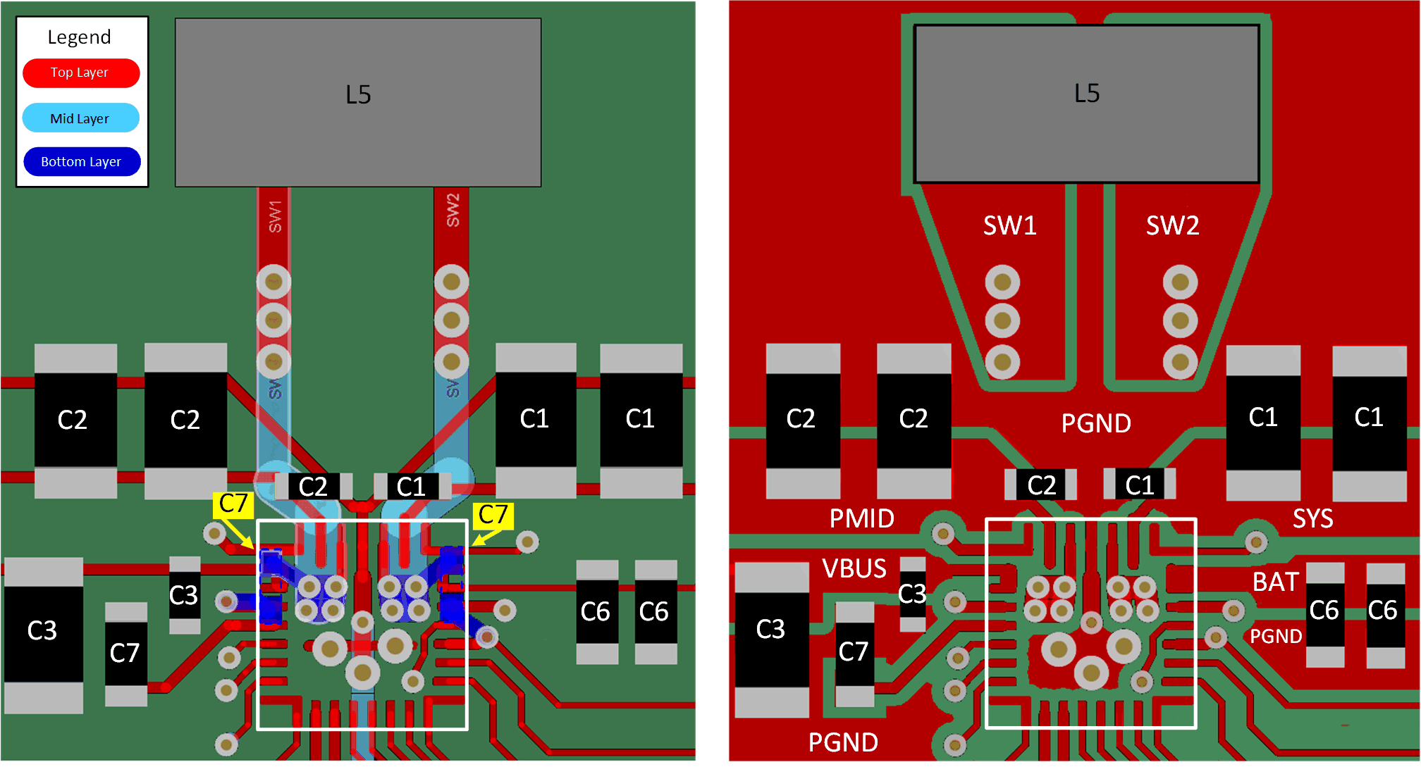
GUID-20200919-CA0I-ZD3L-LTJC-H5M0H9FXW4HC-low.gif Figure 12-2 PCB Layout Example (Top Layer Copper Pours Removed on Left, Shown on Right)

#GUID-827970A7-2B6D-417F-BF71-833A8334ADB2 shows the recommended placement and routing of external components. The components are labelled with "R," "C" or "L" to indicate resistor, capacitor or inductor and a number that corresponds to the numbered list in GUID-EC8B7A76-7058-4DE6-889A-B5B614077B2C.html. Since the layout guidelines are listed in priority order, this number also provides a priority for component placement.

The placement of C1 and C2 0.1 µF PMID and SYS capacitors is critical for noise filtering. They should be placed on the same layer as the BQ25798, as close to the IC as possible. This will generally require that the traces to connect SW1 and SW2 to the inductor are routed on a different layer.

The SW1 and SW2 pins are routed to vias placed under the IC and then back out on an inner PCB layer. This supports the tightest placement of C1 and C2 capctiors as described above. These vias are also used to route to the C7 BTST1 and BTST2 capactiors on the bottom layer as shown.