ZHCSO21 may 2021 BQ25720
PRODUCTION DATA
- 1
- 1 特性
- 2 应用
- 3 说明
- 4 Revision History
- 5 Description (continued)
- 6 Device Comparison Table
- 7 Pin Configuration and Functions
- 8 Specifications
-
9 Detailed Description
- 9.1 Overview
- 9.2 Functional Block Diagram
- 9.3
Feature Description
- 9.3.1 Power-Up Sequence
- 9.3.2 Vmin Active Protection (VAP) with Battery only
- 9.3.3 Two-Level Battery Discharge Current Limit
- 9.3.4 Fast Role Swap Feature
- 9.3.5 CHRG_OK Indicator
- 9.3.6 Input and Charge Current Sensing
- 9.3.7 Input Voltage and Current Limit Setup
- 9.3.8 Battery Cell Configuration
- 9.3.9 Device HIZ State
- 9.3.10 USB On-The-Go (OTG)
- 9.3.11 Converter Operation
- 9.3.12 Inductance Detection Through IADPT Pin
- 9.3.13 Converter Compensation
- 9.3.14 Continuous Conduction Mode (CCM)
- 9.3.15 Pulse Frequency Modulation (PFM)
- 9.3.16 Switching Frequency and Dithering Feature
- 9.3.17 Current and Power Monitor
- 9.3.18 Input Source Dynamic Power Management
- 9.3.19 Input Current Optimizer (ICO)
- 9.3.20 Two-Level Adapter Current Limit (Peak Power Mode)
- 9.3.21 Processor Hot Indication
- 9.3.22
Device Protection
- 9.3.22.1 Watchdog Timer
- 9.3.22.2 Input Overvoltage Protection (ACOV)
- 9.3.22.3 Input Overcurrent Protection (ACOC)
- 9.3.22.4 System Overvoltage Protection (SYSOVP)
- 9.3.22.5 Battery Overvoltage Protection (BATOVP)
- 9.3.22.6 Battery Discharge Overcurrent Protection (BATOC)
- 9.3.22.7 Battery Short Protection (BATSP)
- 9.3.22.8 System Undervoltage Lockout (VSYS_UVP) and Hiccup Mode
- 9.3.22.9 Thermal Shutdown (TSHUT)
- 9.4 Device Functional Modes
- 9.5 Programming
- 9.6
Register Map
- 9.6.1 ChargeOption0 Register (SMBus address = 12h) [reset = E70Eh]
- 9.6.2 ChargeCurrent Register (SMBus address = 14h) [reset = 0000h]
- 9.6.3 ChargeVoltage Register (SMBus address = 15h) [reset value based on CELL_BATPRESZ pin setting]
- 9.6.4 ChargerStatus Register (SMBus address = 20h) [reset = 0000h]
- 9.6.5 ProchotStatus Register (SMBus address = 21h) [reset = B800h]
- 9.6.6 IIN_DPM Register With 10-mΩ Sense Resistor (SMBus address = 22h) [reset = 4100h]
- 9.6.7 ADCVBUS/PSYS Register (SMBus address = 23h)
- 9.6.8 ADCIBAT Register (SMBus address = 24h)
- 9.6.9 ADCIINCMPIN Register (SMBus address = 25h)
- 9.6.10 ADCVSYSVBAT Register (SMBus address = 26h)
- 9.6.11 ChargeOption1 Register (SMBus address = 30h) [reset = 3300h]
- 9.6.12 ChargeOption2 Register (SMBus address = 31h) [reset = 00B7]
- 9.6.13 ChargeOption3 Register (SMBus address = 32h) [reset = 0434h]
- 9.6.14 ProchotOption0 Register (SMBus address = 33h) [reset = 4A81h(2S~) 4A09(1S)]
- 9.6.15 ProchotOption1 Register (SMBus address = 34h) [reset = 41A0h]
- 9.6.16 ADCOption Register (SMBus address = 35h) [reset = 2000h]
- 9.6.17 ChargeOption4 Register (SMBus address = 36h) [reset = 0048h]
- 9.6.18 Vmin Active Protection Register (SMBus address = 37h) [reset = 006Ch(2s~4s)/0004h(1s)]
- 9.6.19 OTGVoltage Register (SMBus address = 3Bh) [reset = 09C4h]
- 9.6.20 OTGCurrent Register (SMBus address = 3Ch) [reset = 3C00h]
- 9.6.21 InputVoltage (VINDPM) Register (SMBus address = 3Dh) [reset = VBUS-1.28V]
- 9.6.22 VSYS_MIN Register (SMBus address = 3Eh) [reset value based on CELL_BATPRESZ pin setting]
- 9.6.23 IIN_HOST Register (SMBus address = 3Fh) [reset = 4100h]
- 9.6.24 ID Registers
- 10Application and Implementation
- 11Power Supply Recommendations
- 12Layout
- 13Device and Documentation Support
- 14Mechanical, Packaging, and Orderable Information
10.2.3 Application Curves
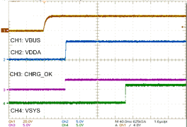
| 2-cell without battery | ||
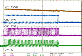
| 3-cell VBAT = 10 V |
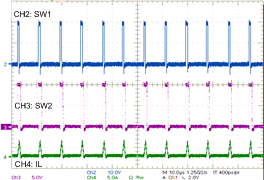
| VBUS = 20 V, VSYS = 10 V, ISYS = 200 mA |
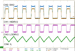
| VBUS = 5 V, VBAT = 10 V |
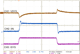
| VBUS = 12 V/3.25 A, 3-cell, VSYS = 9 V, Without battery |
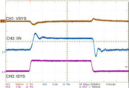
| VBUS = 5 V/3.25 A, 3-cell, VSYS = 9 V, Without battery |
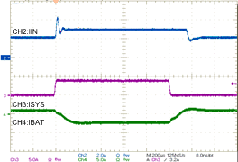
| VBUS = 5 V/3.25 A, VBAT = 7.5 V |
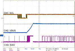
| VBAT = 10 V, VBUS 5 V to 20 V, IOTG = 500 mA |
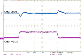
| VBAT = 10 V, VBUS = 20 V |
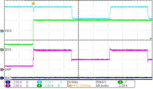
| VBUS = 20 V | IIN_DPM = 2 A | ILIM2_VTH = 200% |
| TMAX = 20 ms | TOVLD = 10 ms | VSYS_MIN = 12.3 V |
| ISYS = 1 to 6 A | ICHG = 0 A |
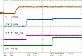
| 2-cell without battery | ||
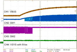
| VBUS 5 V to 20 V |
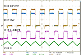
| VBUS = 20 V, VSYS = 10 V, ISYS = 2 A |
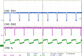
| VBUS = 12 V, VBAT = 12 V |
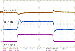
| VBUS = 9 V/3.25 A, 3-cell, VSYS = 9 V, Without battery |
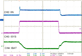
| VBUS = 20 V/3.25 A, VBAT = 7.5 V |
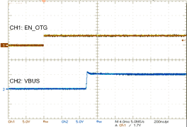
| VBUS = 5 V |
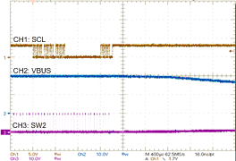
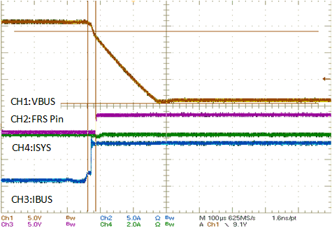
| VBUS = 20 V, VOTG = 5 V, ISYS = 5 A,VBAT = 14.8 V |
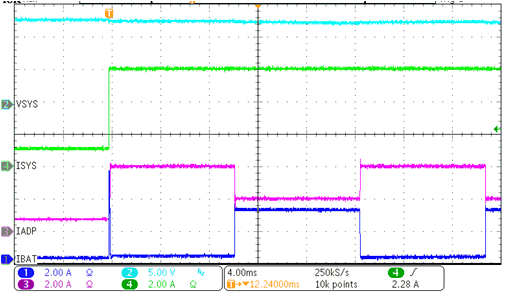
| VBUS = 20 V | IIN_DPM = 2 A | ILIM2_VTH = 200% |
| TMAX = 20 ms | TOVLD = 10 ms | VBAT = 12.8 V |
| ISYS = 1 to 6 A | ICHG = 0 A |