ZHCSO49C May 2021 – March 2023 TPS629210-Q1
PRODUCTION DATA
- 1 特性
- 2 应用
- 3 说明
- 4 Revision History
- 5 Device Comparison Table
- 6 Pin Configuration and Functions
- 7 Specifications
-
8 Detailed Description
- 8.1 Overview
- 8.2 Functional Block Diagram
- 8.3
Feature Description
- 8.3.1 Mode Selection and Device Configuration (MODE/S-CONF Pin)
- 8.3.2 Adjustable VO Operation (External Voltage Divider)
- 8.3.3 Selectable VO Operation (VSET and Internal Voltage Divider)
- 8.3.4 Smart Enable with Precise Threshold
- 8.3.5 Power Good (PG)
- 8.3.6 Output Discharge Function
- 8.3.7 Undervoltage Lockout (UVLO)
- 8.3.8 Current Limit and Short Circuit Protection
- 8.3.9 Thermal Shutdown
- 8.4 Device Functional Modes
- 9 Application and Implementation
- 10Device and Documentation Support
- 11Mechanical, Packaging, and Orderable Information
8.3.1 Mode Selection and Device Configuration (MODE/S-CONF Pin)
The MODE/S-CONF pin is an input with two functions, which can be used to customize the device behavior in two ways:
- Select the device mode (forced PWM or auto PFM/PWM operation) traditionally with a HIGH or LOW level.
- Select the device configuration (switching frequency, internal and external feedback, output discharge, and PFM/PWM mode) by connecting a single resistor to this pin.
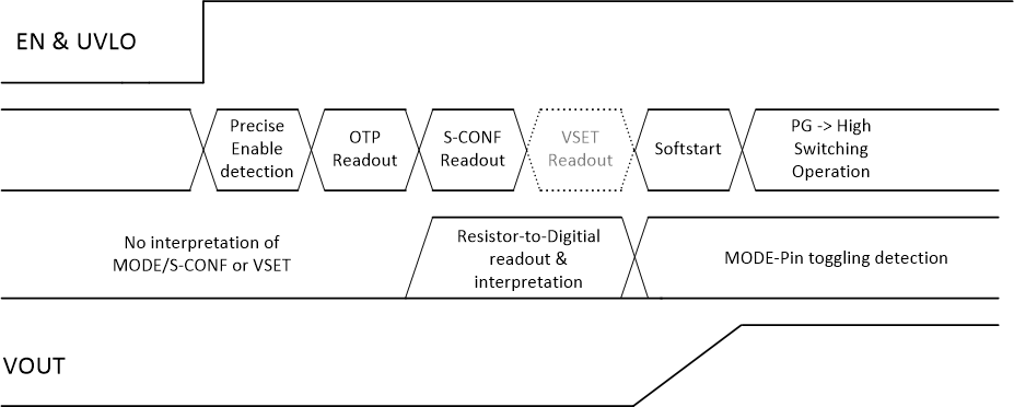
The device interprets this pin during its start-up sequence after the internal OTP readout and before it starts switching in soft start. If the device reads a HIGH or LOW level, dynamic mode change is active and PFM/PWM mode can be changed during operation. If the device reads a resistor value, there is no further interpretation during operation and the device mode or other configurations cannot be changed afterward.
 Figure 8-1 Interpretation of S-CONF and VSET
Flow
Figure 8-1 Interpretation of S-CONF and VSET
FlowTable 8-1 Smart-CONFIG
Setting Table
| # | M ODE/S-CONF Level Or Resistor Value [Ω] (1) | FB/VSET Pin | FSW (MHz) | Output Discharge | Mode (Auto Or Forced PWM) | Dynamic Mode Change |
|---|---|---|---|---|---|---|
| Setting Options by Level | ||||||
| 1 | GND | external FB | up to 2.5(2) | yes | Auto PFM/PWM with AEE | Active |
| 2 | HIGH (> 1.8 V) | external FB | 2.5 | yes | Forced PWM | |
| Setting Options by Resistor | ||||||
| 3 | 7.50 k | external FB | up to 2.5(2) | no | Auto PFM/PWM with AEE | not active |
| 4 | 9.31 k | external FB | 2.5 | no | Forced PWM | |
| 5 | 11.50 k | external FB | 1 | yes | Auto PFM/PWM | |
| 6 | 14.30 k | external FB | 1 | yes | Forced PWM | |
| 7 | 17.80 k | external FB | 1 | no | Auto PFM/PWM | |
| 8 | 22.10 k | external FB | 1 | no | Forced PWM | |
| 9 | 27.40 k | VSET | up to 2.5(2) | yes | Auto PFM/PWM with AEE | |
| 10 | 34.00 k | VSET | 2.5 | yes | Forced PWM | |
| 11 | 42.20 k | VSET | up to 2.5(2) | no | Auto PFM/PWM with AEE | |
| 12 | 52.30 k | VSET | 2.5 | no | Forced PWM | |
| 13 | 64.90 k | VSET | 1 | yes | Auto PFM/PWM | |
| 14 | 80.60 k | VSET | 1 | yes | Forced PWM | |
| 15 | 100.00 k | VSET | 1 | no | Auto PFM/PWM | |
| 16 | 124.00 k | VSET | 1 | no | Forced PWM | |
(1) E96 Resistor Series, 1% accuracy,
temperature coefficient better or equal than ±200 ppm/°C
(2) FSW varies based on
VIN and VOUT. See Section 8.4.3 for more details.