ZHCSO52 June 2021 TMUX646
PRODUCTION DATA
- 1 特性
- 2 应用
- 3 说明
- 4 Revision History
- 5 Pin Configuration and Functions
- 6 Specifications
- 7 Parameter Measurement Information
- 8 Detailed Description
- 9 Application and Implementation
- 10Power Supply Recommendations
- 11Layout
- 12Device and Documentation Support
- 13Mechanical, Packaging, and Orderable Information
7 Parameter Measurement Information
Figure 7-1 On Resistance
Figure 7-2 Off Leakage
Figure 7-3 On Leakage
A. All input pulses are supplied
by generators having the following characteristics: PRR ≤ 10 MHz,
ZO = 50 Ω , tr = 3 ns, tf = 3
ns.
B. CL includes probe
and jig capacitance.
Figure 7-4 tSWITCH
TimingA. All input pulses are supplied
by generators having the following characteristics: PRR ≤ 10 MHz,
ZO = 50 Ω , tr = 3 ns, tf = 3
ns.
B. CL includes probe
and jig capacitance.
Figure 7-5 tON and
tOFF Timing for OE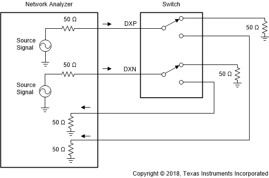 Figure 7-6 Off Isolation
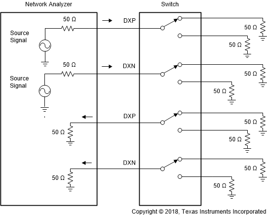 Figure 7-7 Crosstalk
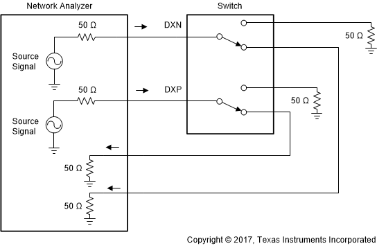 Figure 7-8 Bandwidth and Insertion
Loss
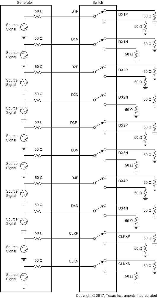 Figure 7-9 tPD,
tSKEW(INTRA) and tSKEW(INTER) Setup
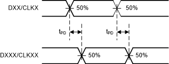
A. All input pulses are supplied
by generators having the following characteristics: PRR ≤ 10 MHz,
ZO = 50 Ω , tr = 100 ps, tf = 100
ps.
B. CL includes probe
and jig capacitance.
Figure 7-10 tPD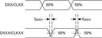
A. All input pulses are
supplied by generators having the following characteristics: PRR ≤ 10 MHz,
ZO = 50 Ω , tr = 100 ps, tf = 100
ps.
B. CL includes probe
and jig capacitance.
Figure 7-11 tSKEW(INTRA)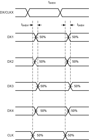
A. All input pulses are
supplied by generators having the following characteristics: PRR ≤ 10 MHz,
ZO = 50 Ω , tr = 100 ps, tf = 100
ps.
B. CL includes probe
and jig capacitance.
C. tSKEW is the maximum skew between all
channels. The diagram exaggerates tSKEW to show the measurement
technique.
Figure 7-12 tSKEW(INTER)A. All input pulses are supplied
by generators having the following characteristics: PRR ≤ 10 MHz,
ZO = 50 Ω , tr = 3 ns, tf = 3
ns.
B. CL includes probe
and jig capacitance.
Figure 7-13 tBBM