ZHCSO52 June 2021 TMUX646
PRODUCTION DATA
- 1 特性
- 2 应用
- 3 说明
- 4 Revision History
- 5 Pin Configuration and Functions
- 6 Specifications
- 7 Parameter Measurement Information
- 8 Detailed Description
- 9 Application and Implementation
- 10Power Supply Recommendations
- 11Layout
- 12Device and Documentation Support
- 13Mechanical, Packaging, and Orderable Information
8.3.3 Powered-Off Protection
When the TMUX646 is powered off (VDD = 0 V) the I/Os and digital logic pins of the device remains in a high impedance state. The crosstalk, off-isolation, and leakage will remain within the electrical specifications. This prevents errant voltages from reaching the rest of the system and maintains isolation when the system is powering up:
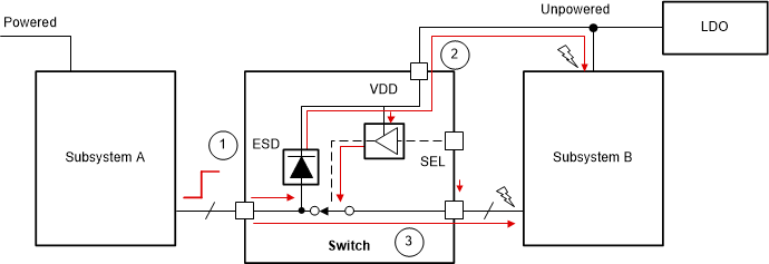
Figure 8-1 shows an example system containing a switch without powered-off protection with the following system level scenario.
- Subsystem A powers up and starts sending information to Subsystem B that remains unpowered.
- The I/O voltage back powers the supply rail in Subsystem B.
- The digital logic is back powered and turns on the switch. The signal is transmitted to Subsystem B before it is powered and damages it.
 Figure 8-1 System Without Powered-Off Protection
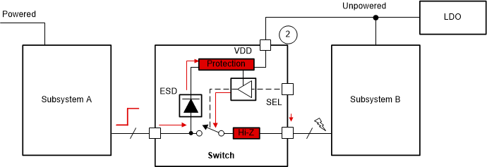
With powered-off protection, the switch prevents back powering the supply and the switch remains high-impedance. Subsystem B remains protected.
 Figure 8-2 System With Powered-Off Protection
This features has the following system level benefits:
- Protects the system from damage.
- Prevents data from being transmitted unintentionally.
- Eliminates the need for power sequencing solutions, reducing BOM count and cost, simplifying system design, and improving reliability.