ZHCSO54A May 2021 – November 2021 CC1352P7
PRODUCTION DATA
- 1 特性
- 2 应用
- 3 说明
- 4 Revision History
- 5 Device Comparison
- 6 Terminal Configuration and Functions
-
7 Specifications
- 7.1 Absolute Maximum Ratings
- 7.2 ESD Ratings
- 7.3 Recommended Operating Conditions
- 7.4 Power Supply and Modules
- 7.5 Power Consumption - Power Modes
- 7.6 Power Consumption - Radio Modes
- 7.7 Nonvolatile (Flash) Memory Characteristics
- 7.8 Thermal Resistance Characteristics
- 7.9 RF Frequency Bands
- 7.10 861 MHz to 1054 MHz - Receive (RX)
- 7.11 861 MHz to 1054 MHz - Transmit (TX)
- 7.12 861 MHz to 1054 MHz - PLL Phase Noise Wideband Mode
- 7.13 861 MHz to 1054 MHz - PLL Phase Noise Narrowband Mode
- 7.14 Bluetooth Low Energy - Receive (RX)
- 7.15 Bluetooth Low Energy - Transmit (TX)
- 7.16 Zigbee and Thread - IEEE 802.15.4-2006 2.4 GHz (OQPSK DSSS1:8, 250 kbps) - RX
- 7.17 Zigbee and Thread - IEEE 802.15.4-2006 2.4 GHz (OQPSK DSSS1:8, 250 kbps) - TX
- 7.18 Timing and Switching Characteristics
- 7.19 Peripheral Characteristics
- 7.20 Typical Characteristics
- 8 Detailed Description
- 9 Application, Implementation, and Layout
- 10Device and Documentation Support
- 11Mechanical, Packaging, and Orderable Information
7.20.3 TX Current
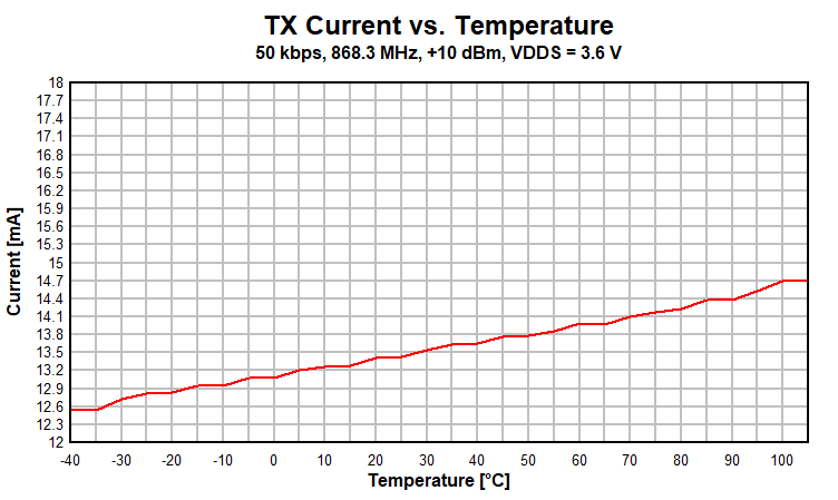
 Figure 7-10 TX Current vs. Temperature (50 kbps, 868.3 MHz, VDDS = 3.6
V)
Figure 7-10 TX Current vs. Temperature (50 kbps, 868.3 MHz, VDDS = 3.6
V)Figure 7-12 TX
Current vs. Temperature (Bluetooth Low Energy 1 Mbps, 2.44 GHz)
Figure 7-14 TX
Current vs. Temperature (250 kbps, 2.44 GHz, +10 dBm PA)
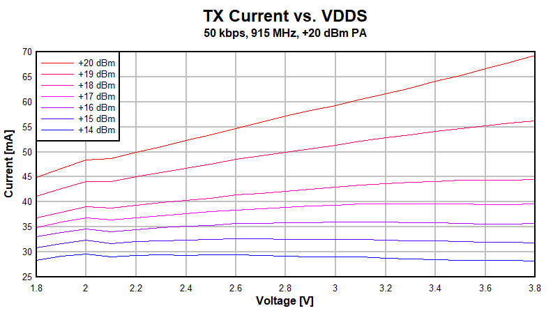
 Figure 7-16 TX Current vs. Supply Voltage (VDDS) (50 kbps, 915 MHz)
Figure 7-18 TX
Current vs. Supply Voltage (VDDS) (Bluetooth Low Energy 1 Mbps, 2.44 GHz,
+20 dBm PA)
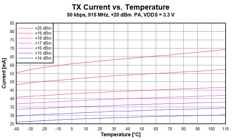
 Figure 7-11 TX Current vs. Temperature (50 kbps, 915 MHz, VDDS = 3.3
V)
Figure 7-11 TX Current vs. Temperature (50 kbps, 915 MHz, VDDS = 3.3
V)Figure 7-13 TX
Current vs. Temperature (Bluetooth Low Energy 1 Mbps, 2.44 GHz, VDDS = 3.3
V)
 Figure 7-15 TX Current vs. Supply Voltage (VDDS) (50 kbps, 868.3 MHz)
Figure 7-17 TX Current vs. Supply
Voltage (VDDS) (Bluetooth Low Energy 1 Mbps, 2.44 GHz)
Figure 7-19 TX
Current vs. Supply Voltage (VDDS) (250 kbps, 2.44 GHz, +10 dBm PA)
Table 7-1 and Table 7-5Table 7-3 show typical TX current and output power for different output power settings.
Table 7-1 Typical TX Current and Output Power
| CC1352P7 at 868 MHz, VDDS = 3.6 V (1) (Measured on CC1352P-7EM-XD7793-XD24-PA9093) | |||
|---|---|---|---|
| txPower | TX Power Setting (SmartRF Studio) | Typical Output Power [dBm] | Typical Current Consumption [mA] |
| 0x013F(1) | 14 | 13.6 | 24 |
| 0xB224 | 12.5 | 11.9 | 17 |
| 0x895E | 12 | 11.5 | 16 |
| 0x669A | 11 | 10.6 | 15 |
| 0x3E92 | 10 | 9.7 | 14 |
| 0x3EDC | 9 | 8.9 | 13 |
| 0x2CD8 | 8 | 8.3 | 12 |
| 0x26D4 | 7 | 7.4 | 11 |
| 0x20D1 | 6 | 6.3 | 10 |
| 0x1CCE | 5 | 4.8 | 10 |
| 0x16CD | 4 | 4.2 | 9 |
| 0x14CB | 3 | 2.8 | 8 |
| 0x12CA | 2 | 1.9 | 8 |
| 0x12C9 | 1 | 1.0 | 8 |
| 0x10C8 | 0 | -0.1 | 7 |
| 0x0AC4 | -5 | -6.8 | 6 |
| 0x0AC2 | -10 | -13.3 | 5 |
| 0x06C1 | -15 | -18.5 | 5 |
| 0x04C0 | -20 | -22.0 | 4 |
(1) Internal regulated voltage powers the PA, therefore the
output power is not affected by variation in VDDS voltage.
Table 7-2 Typical TX Current and Output Power
| CC1352P7 at 915 MHz, VDDS = 3.3 V (1) (Measured on CC1352P-7EM-XD7793-XD24-PA9093) | |||
|---|---|---|---|
| txPower | TX Power Setting (SmartRF Studio) | Typical Output Power [dBm] | Typical Current Consumption [mA] |
| 0x1B8ED2 | 20 | 20.4 | 65 |
| 0x448CF | 19 | 19.3 | 55 |
| 0x48022 | 18 | 17.8 | 45 |
| 0x2661C | 17 | 16.8 | 41 |
| 0x5618 | 16 | 15.9 | 37 |
| 0x4812 | 15 | 14.9 | 33 |
| 0x380D | 14 | 13.7 | 30 |
(1) VDDS powers the PA, therefore the output power is affected
by variation in VDDS voltage.
Table 7-3 Typical TX Current and Output Power
| CC1352P7 at 2.4 GHz, VDDS = 3.3 V (1) (Measured on CC1352-7PEM-XD7793-XD24-PA24) | |||
|---|---|---|---|
| txPower | TX Power Setting (SmartRF Studio) | Typical Output Power [dBm] | Typical Current Consumption [mA] |
| 0x3F75F5 | 20 | 19.6 | 102 |
| 0x3F61E2 | 19 | 18.3 | 86 |
| 0x3047E0 | 18 | 17.4 | 79 |
| 0x1B4FE5 | 17 | 16.3 | 71 |
| 0x1B39DE | 16 | 15.2 | 63 |
| 0x1B2FDA | 15 | 14.3 | 58 |
| 0x1B27D6 | 14 | 13.2 | 52 |
(1) VDDS powers the PA, therefore the output power is affected
by variation in VDDS voltage.
Table 7-4 Typical TX Current and Output Power
| CC1352P7 at 2.4 GHz, VDDS = 3.0 V (1) (Measured on CC1352-7PEM-XD7793-XD24-PA24_10dBm) | |||
|---|---|---|---|
| txPower | TX Power Setting (SmartRF Studio) | Typical Output Power [dBm] | Typical Current Consumption [mA] |
| 0x103F5F | 10 | 10.7 | 21 |
| 0x10335A | 9 | 9.6 | 19 |
| 0x143661 | 8 | 8.5 | 19 |
| 0x144F2A | 7 | 7.6 | 17 |
| 0x144F26 | 6 | 6.6 | 16 |
| 0x144722 | 5 | 5.4 | 15 |
(1) Internal regulated voltage powers the PA, therefore the
output power is not affected by variation in VDDS voltage.
Table 7-5 Typical TX Current and Output
Power
| CC1352P7 at 2.4 GHz, VDDS = 3.0 V (1) (Measured on CC1352-7PEM-XD7793-XD24-PA24) | |||
|---|---|---|---|
| txPower | TX Power Setting (SmartRF Studio) | Typical Output Power [dBm] | Typical Current Consumption [mA] |
| 0x762E | 5 | 4.7 | 10 |
| 0x8220 | 4 | 3.7 | 9 |
| 0x5617 | 3 | 2.8 | 8 |
| 0x3E66 | 2 | 1.9 | 8 |
| 0x3261 | 1 | 0.9 | 8 |
| 0x2C5D | 0 | 0.0 | 7 |
| 0x1899 | -3 | -3.1 | 6 |
| 0x1695 | -5 | -4.9 | 6 |
| 0x1693 | -6 | -6.0 | 6 |
| 0x0CD4 | -9 | -9.1 | 5 |
| 0x0AD3 | -10 | -9.8 | 5 |
| 0x0AD0 | -12 | -11.9 | 5 |
| 0x06CD | -15 | -14.6 | 5 |
| 0x04CA | -18 | -17.8 | 5 |
| 0x04C8 | -20 | -20.4 | 4 |
(1) Internal regulated voltage powers the PA, therefore the
output power is not affected by variation in VDDS voltage.
1. Boost mode enabled. VDDR regulated to 1.95
V.