ZHCSOO3A May   2021  – December 2021

PRODUCTION DATA  

  1. 特性
  2. 应用
  3. 说明
  4. Revision History
  5. 说明(续)
  6. Pin Configurations and Functions
  7. Specifications
    1. 7.1 Absolute Maximum Ratings
    2. 7.2 ESD Ratings
    3. 7.3 ESD Ratings IEC Specification
    4. 7.4 Recomended Operating Conditions
    5. 7.5 Thermal Information
    6. 7.6 Power Supply Characteristics
    7. 7.7 Electrical Characteristics
    8. 7.8 Switching Characteristics
    9. 7.9 Typical Characteristics
  8. Parameter Measurement Information
  9. Detailed Description
    1. 9.1 Overview
    2. 9.2 Functional Block Diagram
    3. 9.3 Feature Description
      1. 9.3.1  VSUP Pin
      2. 9.3.2  VFLT Pin
      3. 9.3.3  Digital Inputs and Outputs
        1. 9.3.3.1 TXD Pin
        2. 9.3.3.2 RXD Pin
        3. 9.3.3.3 TS Pin
      4. 9.3.4  Digital Control and Timing
      5. 9.3.5  VIO Pin
      6. 9.3.6  GND
      7. 9.3.7  INH Pin
      8. 9.3.8  WAKE Pin
      9. 9.3.9  CAN Bus Pins
      10. 9.3.10 Local Faults
        1. 9.3.10.1 TXD Dominant Timeout (TXD DTO)
        2. 9.3.10.2 Thermal Shutdown (TSD)
        3. 9.3.10.3 Under/Over Voltage Lockout
        4. 9.3.10.4 Unpowered Devices
        5. 9.3.10.5 Floating Terminals
        6. 9.3.10.6 CAN Bus Short Circuit Current Limiting
        7. 9.3.10.7 Sleep Wake Error Timer
    4. 9.4 Device Functional Modes
      1. 9.4.1 Operating Mode Description
        1. 9.4.1.1 Normal Mode
        2. 9.4.1.2 Standby Mode
        3. 9.4.1.3 Sleep Mode
          1. 9.4.1.3.1 Remote Wake Request via Wake-Up Pattern (WUP)
          2. 9.4.1.3.2 Local Wake-Up (LWU) via WAKE Input Terminal
        4. 9.4.1.4 Fail-safe Mode
      2. 9.4.2 CAN Transceiver
        1. 9.4.2.1 CAN Transceiver Operation
        2. 9.4.2.2 CAN Transceiver Modes
          1. 9.4.2.2.1 CAN Off Mode
          2. 9.4.2.2.2 CAN Autonomous: Inactive and Active
          3. 9.4.2.2.3 CAN Active
        3. 9.4.2.3 Driver and Receiver Function Tables
        4. 9.4.2.4 CAN Bus States
  10. 10Application Information
    1. 10.1 Application Information Disclaimer
    2. 10.2 Typical Application
      1. 10.2.1 Design Requirements
        1. 10.2.1.1 Bus Loading, Length and Number of Nodes
      2. 10.2.2 Detailed Design Procedures
        1. 10.2.2.1 CAN Termination
    3. 10.3 Application Curves
  11. 11Power Supply Requirements
  12. 12Layout
    1. 12.1 Layout Guidelines
    2. 12.2 Layout Example
  13. 13Device and Documentation Support
    1. 13.1 Documentation Support
      1. 13.1.1 Related Documentation
    2. 13.2 接收文档更新通知
    3. 13.3 支持资源
    4. 13.4 Trademarks
    5. 13.5 Electrostatic Discharge Caution
    6. 13.6 术语表
  14. 14Mechanical, Packaging, and Orderable Information
Local Wake-Up (LWU) via WAKE Input Terminal

The WAKE terminal is a bi-directional high-voltage reverse battery protected input which can be used for local wake-up (LWU) requests via a voltage transition. A LWU event is triggered on either a low-to-high or high-to-low transition since it has bi-directional input thresholds. The WAKE pin could be used with a switch to VSUP or to ground. If the terminal is unused, it should be pulled to VSUP or ground to avoid unwanted parasitic wake-up events.
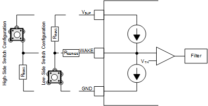
GUID-6A84F143-6C38-4E45-90AB-043D6259DFE1-low.pngFigure 9-5 WAKE Circuit Example

Figure 9-5 shows two possible configurations for the WAKE pin, a low-side and high-side switch configuration. The objective of the series resistor, RSERIES, is to protect the WAKE input of the device from over current conditions that may occur in the event of a ground shift or ground loss. The minimum value of RSERIES can be calculated using the maximum supply voltage, VSUPMAX, and the maximum allowable current of the WAKE pin, IIO(WAKE). RSERIES is calculated using:

Equation 3. RSERIES = VSUPMAX / IIO(WAKE)

If the battery voltage never exceeds 42 VDC, then the RSERIES value is approximately 10 kΩ.

The RBIAS resistor is used to set the static voltage level of the WAKE input when the switch is not in use. When the switch is in use in a high-side switch configuration, the RBIAS resistor in combination with the RSERIES resistor sets the WAKE pin voltage above the VIH threshold. The maximum value of RBIAS can be calculated using the maximum supply voltage, VSUPMAX, the maximum WAKE threshold voltage VIH, the maximum WAKE input current IIH and the series resistor value RSERIES. RBIAS is calculated using:

Equation 4. RBIAS < ((VSUPMAX - VIH) / IIH) - RSERIES

If the battery voltage never exceed 42 VDC, then the RBIAS resistor value must be less than 650-kΩ.

The LWU circuitry is active in sleep mode.. If a valid LWU event occurs the TCAN1162-Q1 transitions from sleep mode to standby mode..

The WAKE circuitry is switched off normal mode.

The RXD pin is only driven once VIO is present.
Figure 9-6 LWU Request Rising Edge
The RXD pin is only driven once VIO is present.
Figure 9-7 LWU Request Falling Edge