ZHCSOO3A May   2021  – December 2021

PRODUCTION DATA  

  1. 特性
  2. 应用
  3. 说明
  4. Revision History
  5. 说明(续)
  6. Pin Configurations and Functions
  7. Specifications
    1. 7.1 Absolute Maximum Ratings
    2. 7.2 ESD Ratings
    3. 7.3 ESD Ratings IEC Specification
    4. 7.4 Recomended Operating Conditions
    5. 7.5 Thermal Information
    6. 7.6 Power Supply Characteristics
    7. 7.7 Electrical Characteristics
    8. 7.8 Switching Characteristics
    9. 7.9 Typical Characteristics
  8. Parameter Measurement Information
  9. Detailed Description
    1. 9.1 Overview
    2. 9.2 Functional Block Diagram
    3. 9.3 Feature Description
      1. 9.3.1  VSUP Pin
      2. 9.3.2  VFLT Pin
      3. 9.3.3  Digital Inputs and Outputs
        1. 9.3.3.1 TXD Pin
        2. 9.3.3.2 RXD Pin
        3. 9.3.3.3 TS Pin
      4. 9.3.4  Digital Control and Timing
      5. 9.3.5  VIO Pin
      6. 9.3.6  GND
      7. 9.3.7  INH Pin
      8. 9.3.8  WAKE Pin
      9. 9.3.9  CAN Bus Pins
      10. 9.3.10 Local Faults
        1. 9.3.10.1 TXD Dominant Timeout (TXD DTO)
        2. 9.3.10.2 Thermal Shutdown (TSD)
        3. 9.3.10.3 Under/Over Voltage Lockout
        4. 9.3.10.4 Unpowered Devices
        5. 9.3.10.5 Floating Terminals
        6. 9.3.10.6 CAN Bus Short Circuit Current Limiting
        7. 9.3.10.7 Sleep Wake Error Timer
    4. 9.4 Device Functional Modes
      1. 9.4.1 Operating Mode Description
        1. 9.4.1.1 Normal Mode
        2. 9.4.1.2 Standby Mode
        3. 9.4.1.3 Sleep Mode
          1. 9.4.1.3.1 Remote Wake Request via Wake-Up Pattern (WUP)
          2. 9.4.1.3.2 Local Wake-Up (LWU) via WAKE Input Terminal
        4. 9.4.1.4 Fail-safe Mode
      2. 9.4.2 CAN Transceiver
        1. 9.4.2.1 CAN Transceiver Operation
        2. 9.4.2.2 CAN Transceiver Modes
          1. 9.4.2.2.1 CAN Off Mode
          2. 9.4.2.2.2 CAN Autonomous: Inactive and Active
          3. 9.4.2.2.3 CAN Active
        3. 9.4.2.3 Driver and Receiver Function Tables
        4. 9.4.2.4 CAN Bus States
  10. 10Application Information
    1. 10.1 Application Information Disclaimer
    2. 10.2 Typical Application
      1. 10.2.1 Design Requirements
        1. 10.2.1.1 Bus Loading, Length and Number of Nodes
      2. 10.2.2 Detailed Design Procedures
        1. 10.2.2.1 CAN Termination
    3. 10.3 Application Curves
  11. 11Power Supply Requirements
  12. 12Layout
    1. 12.1 Layout Guidelines
    2. 12.2 Layout Example
  13. 13Device and Documentation Support
    1. 13.1 Documentation Support
      1. 13.1.1 Related Documentation
    2. 13.2 接收文档更新通知
    3. 13.3 支持资源
    4. 13.4 Trademarks
    5. 13.5 Electrostatic Discharge Caution
    6. 13.6 术语表
  14. 14Mechanical, Packaging, and Orderable Information

CAN Termination

Termination may be a single 120-Ω resistor at the end of the bus on either the cable or in a terminating node. If filtering and stabilization of the common mode voltage of the bus is desired then split termination may used, see Figure 10-2. Split termination improves the electromagnetic emissions behavior of the network by filtering higher-frequency common-mode noise that may be present on the differential signal lines..
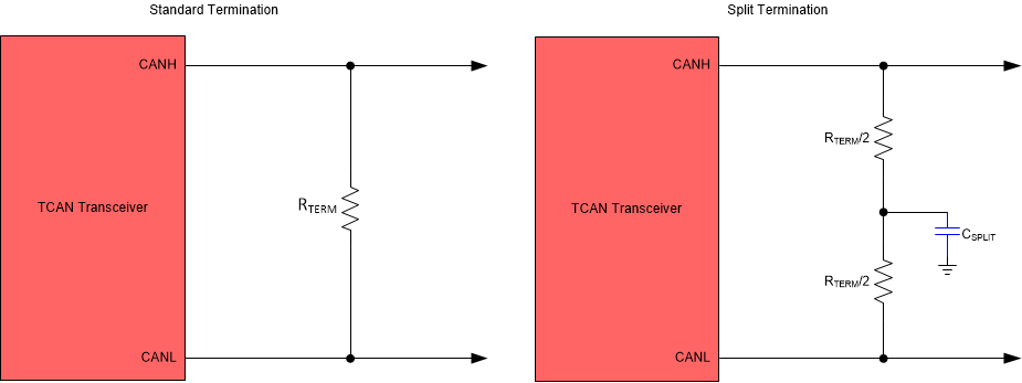
GUID-B1B4E9FE-D7F2-4067-86DE-7A756720FD90-low.gifFigure 10-2 CAN Bus Termination Concepts