ZHCSOO5I April   2004  – November 2023 TPS715A

PRODUCTION DATA  

  1.   1
  2. 特性
  3. 应用
  4. 说明
  5. Pin Configuration and Functions
  6. Specifications
    1. 5.1 Absolute Maximum Ratings
    2. 5.2 ESD Ratings
    3. 5.3 Recommended Operating Conditions
    4. 5.4 Thermal Information
    5. 5.5 Electrical Characteristics
    6. 5.6 Typical Characteristics
  7. Detailed Description
    1. 6.1 Overview
    2. 6.2 Functional Block Diagrams
    3. 6.3 Feature Description
      1. 6.3.1 Wide Supply Range
      2. 6.3.2 Low Supply Current
      3. 6.3.3 Current Limit
      4. 6.3.4 Dropout Voltage (VDO)
    4. 6.4 Device Functional Modes
      1. 6.4.1 Normal Operation
      2. 6.4.2 Dropout Operation
  8. Application and Implementation
    1. 7.1 Application Information
    2. 7.2 Typical Applications
      1. 7.2.1 Design Requirements
      2. 7.2.2 Detailed Design Procedure
        1. 7.2.2.1 Setting VOUT for the TPS715A01 Adjustable LDO
        2. 7.2.2.2 External Capacitor Requirements
        3. 7.2.2.3 Input and Output Capacitor Requirements
        4. 7.2.2.4 Reverse Current
        5. 7.2.2.5 Feed-Forward Capacitor (CFF)
        6. 7.2.2.6 Power Dissipation (PD)
        7. 7.2.2.7 Estimating Junction Temperature
      3. 7.2.3 Application Curves
    3. 7.3 Best Design Practices
    4. 7.4 Power Supply Recommendations
    5. 7.5 Layout
      1. 7.5.1 Layout Guidelines
        1. 7.5.1.1 Power Dissipation
      2. 7.5.2 Layout Example
  9. Device and Documentation Support
    1. 8.1 Device Support
      1. 8.1.1 Development Support
        1. 8.1.1.1 Evaluation Module
        2. 8.1.1.2 Spice Models
      2. 8.1.2 Device Nomenclature
    2. 8.2 Documentation Support
      1. 8.2.1 Related Documentation
    3. 8.3 接收文档更新通知
    4. 8.4 支持资源
    5. 8.5 Trademarks
    6. 8.6 静电放电警告
    7. 8.7 术语表
  10. Revision History
  11. 10Mechanical, Packaging, and Orderable Information

Application Curves

at operating temperature TJ = 25°C, VIN = VOUT(NOM) + 1.0 V or 2.5 V (whichever is greater), IOUT = 1 mA, CIN = 1 µF, and COUT = 1 µF (unless otherwise noted)
GUID-5F82F8D2-1C17-4533-A4C1-C1255278B3CB-low.gif
 
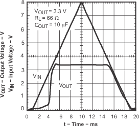
Figure 7-4 Power-Up and Power-Down (Legacy Chip)
GUID-20231024-SS0I-VHMP-CMHZ-L2QRTBZCWRKC-low.svg
 
Figure 7-6 Fast Power-Up (Legacy Chip)
GUID-8D85418D-603F-45D3-917C-B9FACDC064BA-low.gif
 
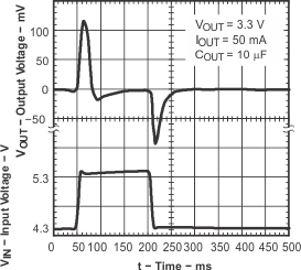
Figure 7-8 Line Transient Response (Legacy Chip)
GUID-CBCE7330-61C7-4A37-B90D-F511CFABA167-low.gif
 
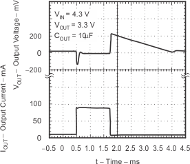
Figure 7-10 Load Transient Response (Legacy Chip)
GUID-20221031-SS0I-F5RN-JNN3-X9BWNZNK1LSJ-low.svg
 
Figure 7-12 Line Transient Response (New Chip)
GUID-20221031-SS0I-SGTH-4LDN-CLLF5TDZ0GKX-low.svg
 
Figure 7-5 Power-Up, Power-Down (New Chip)
GUID-20231024-SS0I-357Q-BR79-QXJZMZVGR0KL-low.svg
 
Figure 7-7 Fast Power-Up (New Chip)
GUID-20221031-SS0I-3BGQ-41JF-7WDRTQFJTZPP-low.svg
 
Figure 7-9 Line Transient Response (New Chip)
GUID-20231024-SS0I-LRBR-C3CX-S44T98HWD7GD-low.svg
 
Figure 7-11 Load Transient Response (New Chip)
GUID-5A86EFD3-DBBA-4469-A70C-4105BD77F8CF-low.svg
 
Figure 7-13 Dropout Exit Transient Response (New Chip)