ZHCSP22B october 2021 – march 2023 TMUX8211 , TMUX8212 , TMUX8213
PRODUCTION DATA
- 1 特性
- 2 应用
- 3 说明
- 4 Revision History
- 5 Device Comparison Table
- 6 Pin Configuration and Functions
-
7 Specifications
- 7.1 Absolute Maximum Ratings: TMUX821x Devices
- 7.2 ESD Ratings
- 7.3 Recommended Operating Conditions: TMUX821x Devices
- 7.4 漏极持续电流源
- 7.5 漏极脉冲电流源
- 7.6 Thermal Information
- 7.7 Electrical Characteristics (Global): TMUX821x Devices
- 7.8 Electrical Characteristics (±15-V Dual Supply)
- 7.9 Electrical Characteristics (±36-V Dual Supply)
- 7.10 Electrical Characteristics (±50-V Dual Supply)
- 7.11 Electrical Characteristics (72-V Single Supply)
- 7.12 Electrical Characteristics (100-V Single Supply)
- 7.13 Switching Characteristics: TMUX821x Devices
- 7.14 Typical Characteristics
- 8 Parameter Measurement Information
- 9 Detailed Description
- 10Application and Implementation
- 11Power Supply Recommendations
- 12Layout
- 13Device and Documentation Support
- 14Mechanical, Packaging, and Orderable Information
8.1 On-Resistance
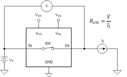
The On-Resistance of the TMUX821x is the ohmic resistance across the source (Sx) and drain (Dx) pins of the device. The On-Resistance varies with input voltage and supply voltage. The symbol RON is used to denote On-Resistance. Figure 8-1 shows the measurement setup used to measure RON. ΔRON represents the difference between the RON of any two channels, while RON_FLAT denotes the flatness that is defined as the difference between the maximum and minimum value of On-Resistance measured over the specified analog signal range.
 Figure 8-1 On-Resistance Measurement Setup