ZHCSP35A December   2021  – September 2022 TPS7A21

PRODUCTION DATA  

  1. 特性
  2. 应用
  3. 说明
  4. Revision History
  5. Pin Configuration and Functions
  6. Specifications
    1. 6.1 Absolute Maximum Ratings
    2. 6.2 ESD Ratings
    3. 6.3 Recommended Operating Conditions
    4. 6.4 Thermal Information
    5. 6.5 Electrical Characteristics
    6. 6.6 Typical Characteristics
  7. Detailed Description
    1. 7.1 Overview
    2. 7.2 Functional Block Diagram
    3. 7.3 Feature Description
      1. 7.3.1 Smart Enable (EN)
      2. 7.3.2 Low Output Noise
      3. 7.3.3 Active Discharge
      4. 7.3.4 Dropout Voltage
      5. 7.3.5 Foldback Current Limit
      6. 7.3.6 Undervoltage Lockout
      7. 7.3.7 Thermal Overload Protection (TSD)
    4. 7.4 Device Functional Modes
      1. 7.4.1 Device Functional Mode Comparison
      2. 7.4.2 Normal Operation
      3. 7.4.3 Dropout Operation
      4. 7.4.4 Disabled
  8. Applications and Implementation
    1. 8.1 Application Information
      1. 8.1.1 Recommended Capacitor Types
      2. 8.1.2 Input and Output Capacitor Requirements
      3. 8.1.3 Load Transient Response
      4. 8.1.4 Undervoltage Lockout (UVLO) Operation
      5. 8.1.5 Power Dissipation (PD)
      6. 8.1.6 Estimating Junction Temperature
      7. 8.1.7 Recommended Area For Continuous Operation
    2. 8.2 Typical Application
      1. 8.2.1 Design Requirements
      2. 8.2.2 Detailed Design Procedure
        1. 8.2.2.1 Power Dissipation and Device Operation
      3. 8.2.3 Application Curves
    3. 8.3 Power Supply Recommendations
    4. 8.4 Layout
      1. 8.4.1 Layout Guidelines
        1. 8.4.1.1 DSBGA Mounting
        2. 8.4.1.2 DSBGA Light Sensitivity
      2. 8.4.2 Layout Example
  9. Device and Documentation Support
    1. 9.1 Device Support
      1. 9.1.1 Device Nomenclature
    2. 9.2 Documentation Support
      1. 9.2.1 Related Documentation
    3. 9.3 接收文档更新通知
    4. 9.4 支持资源
    5. 9.5 Trademarks
    6. 9.6 Electrostatic Discharge Caution
    7. 9.7 术语表
  10. 10Mechanical, Packaging, and Orderable Information
    1. 10.1 Mechanical Data

Undervoltage Lockout (UVLO) Operation

The UVLO circuit verifies that the device stays disabled before the input supply reaches the minimum operational voltage range, and makes sure that the device shuts down when the input supply collapses. Figure 8-2 shows the UVLO circuit response to various input voltage events. The diagram can be separated into the following parts:

  • Region A: The device does not start until the input reaches the UVLO rising threshold.
  • Region B: Normal operation, regulating device.
  • Region C: Brownout event above the UVLO falling threshold (UVLO rising threshold – UVLO hysteresis). The device remains enabled even if the output falls out of regulation.
  • Region D: Normal operation, regulating device.
  • Region E: Brownout event below the UVLO falling threshold. The device is disabled in most cases and the output falls because of the load and active discharge circuit. The device is re-enabled when the UVLO rising threshold is reached by the input voltage and a normal start-up follows.
  • Region F: Normal operation followed by the input falling to the UVLO falling threshold.
  • Region G: The device is disabled when the input voltage falls below the UVLO falling threshold to 0 V. The output falls because of the load and active discharge circuit.
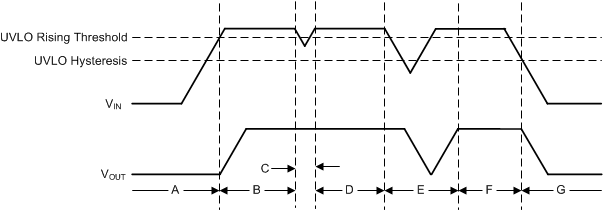
GUID-1A337E3F-D614-48A5-822F-59C20A6A9AF1-low.gif Figure 8-2 Typical UVLO Operation