ZHCSPA5F August 1999 – July 2024 THS4021 , THS4022
PRODUCTION DATA
- 1
- 1 特性
- 2 应用
- 3 说明
- 4 Pin Configuration and Functions
-
5 Specifications
- 5.1 Absolute Maximum Ratings
- 5.2 ESD Ratings
- 5.3 Recommended Operating Conditions
- 5.4 Thermal Information - THS4021
- 5.5 Thermal Information - THS4022
- 5.6 Electrical Characteristics - THS4021D and THS4022DGN
- 5.7 Electrical Characteristics - THS4021DGN
- 5.8 Typical Characteristics: THS4021D and THS4022DGN
- 5.9 Typical Characteristics: THS4021DGN
- 6 Detailed Description
- 7 Application and Implementation
- 8 Device and Documentation Support
- 9 Revision History
- 10Mechanical, Packaging, and Orderable Information
7.1.2 General Configuration
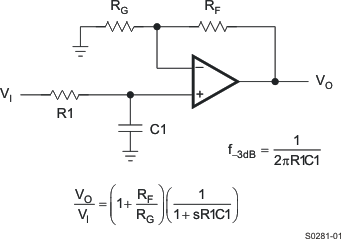
When receiving low-level signals, limiting the bandwidth of the incoming signals into the system is often required. Figure 7-2 shows how the simplest way to accomplish this limiting is to place an RC filter at the noninverting pin of the amplifier.
 Figure 7-2 Single-Pole Low-Pass
Filter