ZHCSPC3A May   2021  – November 2021 TCAN11623-Q1 , TCAN11625-Q1

PRODUCTION DATA  

  1. 特性
  2. 应用
  3. 说明
  4. Revision History
  5. 说明(续)
  6. Pin Configurations and Functions (TCAN11625)
  7. Pin Configurations and Functions (TCAN11623)
  8. Specifications
    1. 8.1 Absolute Maximum Ratings
    2. 8.2 ESD Ratings
    3. 8.3 ESD Ratings IEC Specification
    4. 8.4 Recomended Operating Conditions
    5. 8.5 Thermal Information
    6. 8.6 Power Supply Characteristics
    7. 8.7 Electrical Characteristics
    8. 8.8 Switching Characteristics
    9. 8.9 Typical Characteristics
  9. Parameter Measurement Information
  10. 10Detailed Description
    1. 10.1 Overview
    2. 10.2 Functional Block Diagram
    3. 10.3 Feature Description
      1. 10.3.1  VSUP Pin
      2. 10.3.2  VCCOUT Pin
      3. 10.3.3  VFLT Pin
      4. 10.3.4  VLDO3 Pin
      5. 10.3.5  Digital Inputs and Outputs
        1. 10.3.5.1 TXD Pin
        2. 10.3.5.2 RXD Pin
        3. 10.3.5.3 TS Pin
      6. 10.3.6  Digital Control and Timing
      7. 10.3.7  VIO Pin
      8. 10.3.8  GND
      9. 10.3.9  INH Pin
      10. 10.3.10 WAKE Pin
      11. 10.3.11 nRST Pin
      12. 10.3.12 CAN Bus Pins
      13. 10.3.13 Local Faults
        1. 10.3.13.1 TXD Dominant Timeout (TXD DTO)
        2. 10.3.13.2 Thermal Shutdown (TSD)
        3. 10.3.13.3 Under/Over Voltage Lockout
        4. 10.3.13.4 Unpowered Devices
        5. 10.3.13.5 Floating Terminals
        6. 10.3.13.6 CAN Bus Short Circuit Current Limiting
        7. 10.3.13.7 Sleep Wake Error Timer
    4. 10.4 Device Functional Modes
      1. 10.4.1 Operating Mode Description
        1. 10.4.1.1 Normal Mode
        2. 10.4.1.2 Standby Mode
        3. 10.4.1.3 Sleep Mode
          1. 10.4.1.3.1 Remote Wake Request via Wake-Up Pattern (WUP)
          2. 10.4.1.3.2 Local Wake-Up (LWU) via WAKE Input Terminal
        4. 10.4.1.4 Reset Mode
        5. 10.4.1.5 Fail-safe Mode
      2. 10.4.2 CAN Transceiver
        1. 10.4.2.1 CAN Transceiver Operation
        2. 10.4.2.2 CAN Transceiver Modes
          1. 10.4.2.2.1 CAN Off Mode
          2. 10.4.2.2.2 CAN Autonomous: Inactive and Active
          3. 10.4.2.2.3 CAN Active
        3. 10.4.2.3 Driver and Receiver Function Tables
        4. 10.4.2.4 CAN Bus States
  11. 11Application Information
    1. 11.1 Application Information Disclaimer
    2. 11.2 Typical Application
      1. 11.2.1 Design Requirements
        1. 11.2.1.1 Bus Loading, Length and Number of Nodes
      2. 11.2.2 Detailed Design Procedures
        1. 11.2.2.1 CAN Termination
    3. 11.3 Application Curves
  12. 12Power Supply Requirements
  13. 13Layout
    1. 13.1 Layout Guidelines
    2. 13.2 Layout Example
  14. 14Device and Documentation Support
    1. 14.1 Documentation Support
      1. 14.1.1 Related Documentation
    2. 14.2 接收文档更新通知
    3. 14.3 支持资源
    4. 14.4 Trademarks
    5. 14.5 Electrostatic Discharge Caution
    6. 14.6 术语表
  15. 15Mechanical, Packaging, and Orderable Information

CAN Bus States

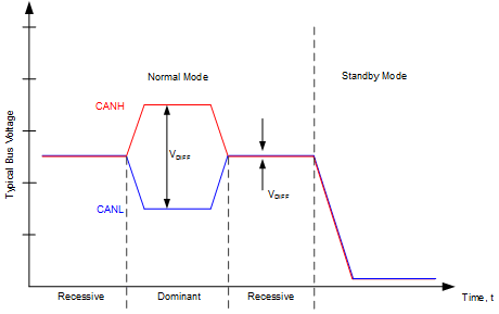
The CAN bus has two logical states during operation: recessive and dominant. See Figure 10-13.

A dominant bus state occurs when the bus is driven differentially and corresponds to a logic low on the TXD and RXD pins. A recessive bus state occurs when the bus is biased to one half of the CAN transceiver supply voltage via the high resistance internal input resistors (RIN) of the receiver and corresponds to a logic high on the TXD and RXD pins.

A dominant state overwrites the recessive state during arbitration. Multiple CAN nodes may be transmitting a dominant bit at the same time during arbitration, and in this case the differential voltage of the CAN bus will be greater than the differential voltage of a single CAN driver. The TCAN1162x-Q1 CAN transceiver implements low-power standby and sleep modes which enables a third bus state where the bus pins are biased to ground via the high resistance internal resistors of the receiver.
GUID-1E531B00-A2FD-436F-8440-CDC52212EE5D-low.gifFigure 10-13 Bus States