ZHCSPI9A December 2021 – December 2022 OPT4001
PRODUCTION DATA
- 1 特性
- 2 应用
- 3 说明
- 4 Revision History
- 5 说明(续)
- 6 Pin Configuration and Functions
- 7 Specifications
- 8 Detailed Description
- 9 Application and Implementation
- 10Device and Documentation Support
- 11Mechanical, Packaging, and Orderable Information
8.4.2 Interrupt Modes of Operation
The device has an interrupt reporting system that allows the processor connected to the I2C bus to go to sleep, or otherwise ignore the device results, until a user-defined event occurs that requires possible action. Alternatively, this same mechanism can also be used with any system that can take advantage of a single digital signal that indicates whether the light is above or below levels of interest.
The INT pin has an open-drain output, which requires the use of a pull-up resistor. This open-drain output allows multiple devices with open-drain INT pins to be connected to the same line, thus creating a logical NOR or AND function between the devices. The polarity of the INT pin can be controlled by the INT_POL.
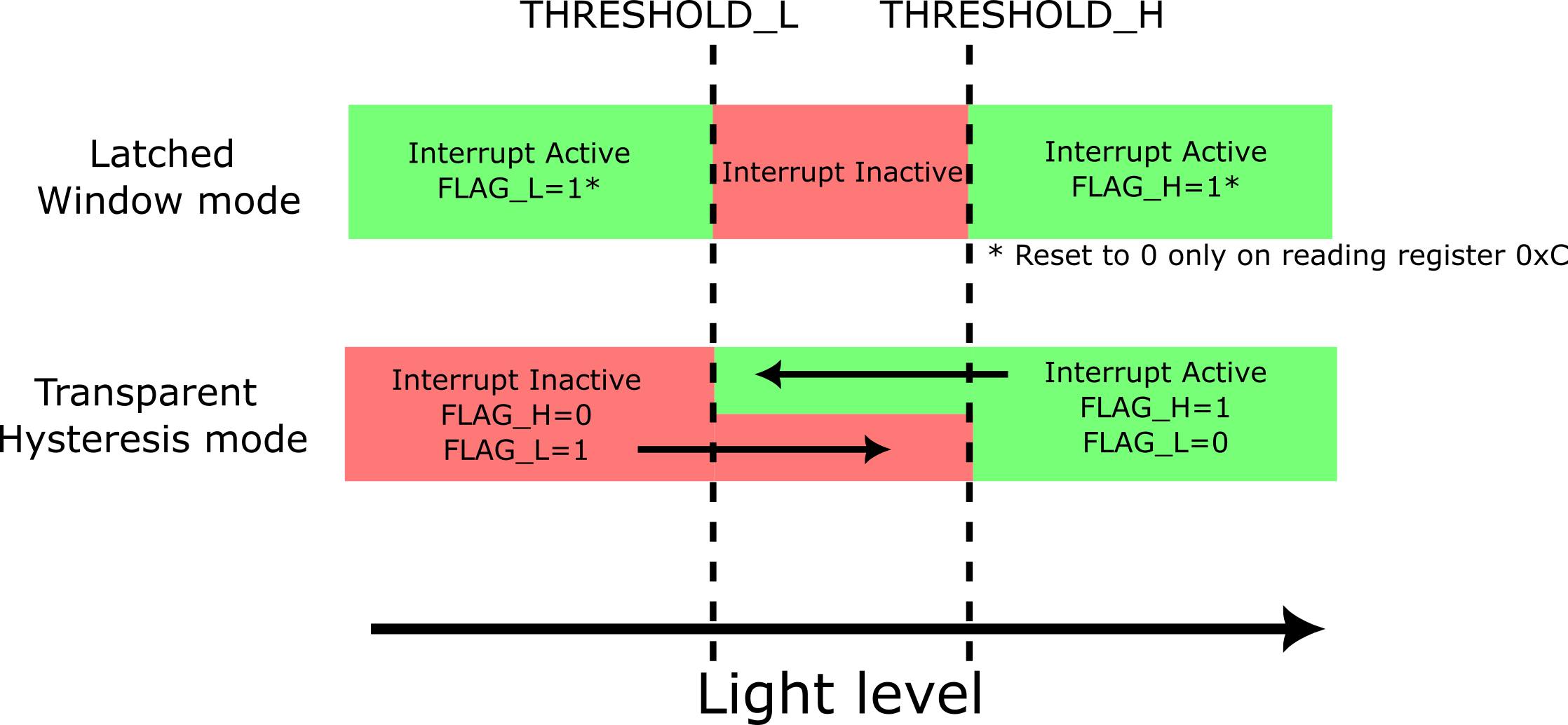
There are two major types of interrupt reporting mechanism modes: latched window comparison mode and transparent hysteresis comparison mode. The configuration register LATCH controls which of these two modes is used. Table 8-1 and Figure 8-4 summarize the function of these two modes. Additionally, the INT pin can either be used to indicate a fault in one of these modes (INT_CFG=0) or to indicate a conversion completion (INT_CFG >0). This is shown in Table 8-2.
 Figure 8-4 Interrupt Pin Status (for
INT_CFG=0 setting) and Register Flag Behavior
 | LATCH Setting | INT Pin State (when INT_CFG=0) | FLAG_H Value | FLAG_L Value | Latching Behavior |
|---|---|---|---|---|
| 0: Transparent hysteresis mode | INT pin indicates if measurement is above (INT active) or below (INT inactive) the threshold. If measurement is between the high and low threshold values then the previous INT value is maintained. This prevents the INT pin from repeated toggling when the measurement values are close to the threshold. | 0: If measurement is below the low
limit 1: If measurement is above the high limit If measurement is between high and low limits previous value is maintained |
0: If measurement is above the
high limit 1: If measurement is below the low limit If measurement is between high and low limits previous value is maintained |
Not latching: Values are updated after each conversion |
| 1: Latched window mode | INT pin becomes active if the measurement is outside the window (above high threshold or below the low threshold). The INT pin does not reset and return to the inactive state until register 0xC is read. | 1: If measurement is above the high limit | 1: If measurement is below the low limit | Latching: INT pin, FLAG_H and FLAG_L values do not reset until the register 0x0C is read. |
The THRESHOLD_H, THRESHOLD_L, LATCH and FAULT_COUNT registers control the interrupt behavior. The LATCH field setting allows a choice between the latched window mode and transparent hysteresis mode as shown in the table. Interrupt reporting can be observed on INT pin (for SOT-5X3 variant only), the FLAG_H, and the FLAG_L registers.
Results from comparing the current sensor measurements with THRESHOLD_H and THRESHOLD_L registers are referred to as fault events. The calculations to set these registers can be found in Threshold Detection Calculations. The FAULT_COUNT register dictates the number of continuous fault events required to trigger an interrupt event and subsequently change the state of the interrupt reporting mechanisms. For example, with a FAULT_COUNT value of 2 corresponding to 4 fault counts, the INT pin (for SOT-5X3 variant only), FLAG_H and FLAG_L states shown in the table are not realized unless 4 consecutive measurements are taken that satisfy the fault condition.
INT pin function (for SOT-5X3 variant only) listed in Table 8-1is valid only when INT_CFG=0. The INT pin function can be changed to indicate an end of conversion or FIFO full state as shown in Table 8-2. The FLAG_H and FLAG_L registers continue to behave as listed in Table 8-1 even while INT_CFG>0. The polarity of the INT pin is controlled by the INT_POL register.
| INT_CFG Setting | INT Pin Function |
|---|---|
| 0 | As per Table 8-1 |
| 1 | INT pin asserted with 1us pulse width after every conversion |
| 3 | INT pin asserted with 1us pulse width every 4 conversions to indicate the FIFO is full |