ZHCSPL6 January 2022 TPS7H4003-SEP
PRODUCTION DATA
- 1 特性
- 2 应用
- 3 说明
- 4 Revision History
- 5 Pin Configuration and Functions
- 6 Specifications
-
7 Detailed Description
- 7.1 Overview
- 7.2 Functional Block Diagram
- 7.3
Feature Description
- 7.3.1 VIN and Power VIN Pins (VIN and PVIN)
- 7.3.2 Voltage Reference
- 7.3.3 Adjusting the Output Voltage
- 7.3.4 Safe Start-Up Into Prebiased Outputs
- 7.3.5 Error Amplifier
- 7.3.6 Enable and Adjust UVLO
- 7.3.7 Adjustable Switching Frequency and Synchronization (SYNC)
- 7.3.8 Soft-Start (SS/TR)
- 7.3.9 Power Good (PWRGD)
- 7.3.10 Sequencing
- 7.3.11 Output Overvoltage Protection (OVP)
- 7.3.12 Overcurrent Protection
- 7.3.13 Thermal Shutdown
- 7.3.14 Turn-On Behavior
- 7.3.15 Slope Compensation
- 7.3.16 Small Signal Model for Frequency Compensation
- 7.4 Device Functional Modes
-
8 Application and Implementation
- 8.1 Application Information
- 8.2
Typical Application
- 8.2.1 Design Requirements
- 8.2.2
Detailed Design Procedure
- 8.2.2.1 Operating Frequency
- 8.2.2.2 Output Inductor Selection
- 8.2.2.3 Output Capacitor Selection
- 8.2.2.4 Output Schottky Diode
- 8.2.2.5 Input Capacitor Selection
- 8.2.2.6 Soft-Start Capacitor Selection
- 8.2.2.7 Undervoltage Lockout (UVLO) Set Point
- 8.2.2.8 Output Voltage Feedback Resistor Selection
- 8.2.2.9 Compensation Component Selection
- 8.2.3 Parallel Operation
- 8.2.4 Application Curve
- 9 Power Supply Recommendations
- 10Layout
- 11Device and Documentation Support
- 12Mechanical, Packaging, and Orderable Information
7.3.7.1 Internal Oscillator Mode
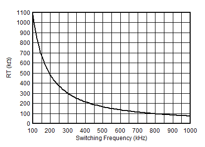
In internal oscillator mode, a resistor is connected between the RT pin and GND to configure the switching frequency, fSW, of the device. The switching frequency is adjustable from 100 kHz to 1 MHz depending on the RT resistor value, which can be calculated using Equation 4. Figure 7-4 shows the relationship curve between the RT resistor value and the configurable switching frequency range. It is recommended that the SYNC2 pin be connected to GND for this mode of operation.
Equation 4.
where
- RT in kΩ
- fSW in kHz
 Figure 7-4 RT vs Switching Frequency