ZHCSPZ0A february   2022  – june 2023 LMK1D1208I

PRODUCTION DATA  

  1.   1
  2. 特性
  3. 应用
  4. 说明
  5. Revision History
  6. Device Comparison
  7. Pin Configuration and Functions
  8. Specifications
    1. 7.1 Absolute Maximum Ratings
    2. 7.2 ESD Ratings
    3. 7.3 Recommended Operating Conditions
    4. 7.4 Thermal Information
    5. 7.5 Electrical Characteristics
    6. 7.6 Typical Characteristics
  9. Parameter Measurement Information
  10. Detailed Description
    1. 9.1 Overview
    2. 9.2 Functional Block Diagram
    3. 9.3 Feature Description
      1. 9.3.1 Fail-Safe Input
      2. 9.3.2 Input Stage Configurability
      3. 9.3.3 Dual Output Bank
      4. 9.3.4 I2C
        1. 9.3.4.1 I2C Address Assignment
      5. 9.3.5 LVDS Output Termination
      6. 9.3.6 Input Termination
    4. 9.4 Device Functional Modes
      1. 9.4.1 Input Enable Control
      2. 9.4.2 Bank Input Selection
      3. 9.4.3 Bank Mute Control
      4. 9.4.4 Output Enable Control
      5. 9.4.5 Output Amplitude Selection
    5. 9.5 Programming
    6. 9.6 Register Maps
      1. 9.6.1 LMK1D1208I Registers
  11. 10Application and Implementation
    1. 10.1 Application Information
    2. 10.2 Typical Application
      1. 10.2.1 Design Requirements
      2. 10.2.2 Detailed Design Procedure
      3. 10.2.3 Application Curves
    3. 10.3 Power Supply Recommendations
    4. 10.4 Layout
      1. 10.4.1 Layout Guidelines
      2. 10.4.2 Layout Example
  12. 11Device and Documentation Support
    1. 11.1 Documentation Support
      1. 11.1.1 Related Documentation
    2. 11.2 接收文档更新通知
    3. 11.3 支持资源
    4. 11.4 Trademarks
    5. 11.5 静电放电警告
    6. 11.6 术语表
  13. 12Mechanical, Packaging, and Orderable Information
    1. 12.1 Package Option Addendum
    2. 12.2 Tape and Reel Information

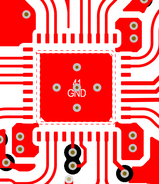
Layout Example

GUID-20211119-SS0I-1TFC-SZ7F-FJPNTFJJSBZL-low.png Figure 10-6 Recommended PCB Layout, Top Layer
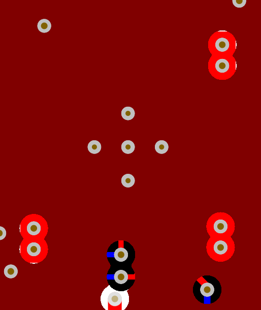
GUID-20211119-SS0I-1GP5-HGKW-NR2JN9QKQ4K7-low.png Figure 10-7 Recommended PCB Layout Bottom Layer