ZHCSQD8C July 2007 – April 2022 PCA9306-Q1
PRODUCTION DATA
- 1 特性
- 2 应用
- 3 说明
- 4 Revision History
- 5 说明(续)
- 6 Pin Configuration and Functions
-
7 Specifications
- 7.1 Absolute Maximum Ratings
- 7.2 ESD Ratings
- 7.3 Recommended Operating Conditions
- 7.4 Thermal Information
- 7.5 Electrical Characteristics
- 7.6 Switching Characteristics: Translating Down, VIH = 3.3 V
- 7.7 Switching Characteristics: Translating Down, VIH = 2.5 V
- 7.8 Switching Characteristics: Translating Up, VIH = 2.3 V
- 7.9 Switching Characteristics: Translating Up, VIH = 1.5 V
- 7.10 Typical Characteristics
- 8 Parameter Measurement Information
-
9 Detailed Description
- 9.1
Overview
- 9.1.1 Definition of threshold voltage
- 9.1.2 Correct Device Set Up
- 9.1.3 Disconnecting a Target from the Main I2C Bus Using the EN Pin
- 9.1.4 Supporting Remote Board Insertion to Backplane with PCA9306-Q1
- 9.1.5 Switch Configuration
- 9.1.6 Controller on Side 1 or Side 2 of Device
- 9.1.7 LDO and PCA9306-Q1 Concerns
- 9.1.8 Current Limiting Resistance on VREF2
- 9.2 Functional Block Diagram
- 9.3 Feature Description
- 9.4 Device Functional Modes
- 9.1
Overview
- 10Application and Implementation
- 11Power Supply Recommendations
- 12Layout
- 13Device and Documentation Support
- 14Mechanical, Packaging, and Orderable Information
9.1.2 Correct Device Set Up
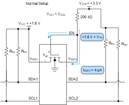
In a normal set up shown in Figure 9-1, the enable pin and VREF2 are shorted together and tied to a 200-kΩ resistor, and a reference voltage equal to VREF1 plus the FET threshold voltage is established. This reference voltage is used to help pass lows from one side to another more effectively while still separating the different pull up voltages on both sides.
 Figure 9-1 Normal Setup
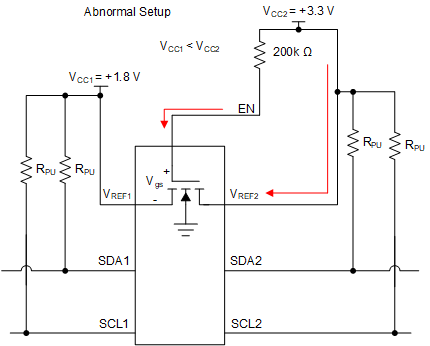
Care should be taken to ensure VREF2 has an external resistor tied between it and VCC2. If VREF2 is tied directly to the VCC2 rail without a resistor, then there is no external resistance from the VCC2 to VCC1 to limit the current such as in Figure 9-2. This effectively looks like a low impedance path for current to travel through and potentially break the pass FET if the current flowing through the pass FET is larger than the absolute maximum continuous channel current specified in section 6.1. The continuous channel current is larger with a higher voltage difference between VCC1 and VCC2.
Figure 9-2 shows an improper set up. If VCC2 is larger than VCC1 but less than Vth, the impedance between VCC1 and VCC2 is high resulting in a low drain to source current, which does not cause damage to the device. Concern arises when VCC2 becomes larger than VCC1 by Vth. During this event, the NFET turns on and begin to conduct current. This current is dependent on the gate to source voltage and drain to source voltage.
 Figure 9-2 Abnormal Setup