ZHCSRC5K september 2003 – april 2023 THS3091 , THS3095
PRODUCTION DATA
- 1 特性
- 2 应用
- 3 描述
- 4 Revision History
- 5 Device Comparison Table
- 6 Pin Configuration and Functions
- 7 Specifications
- 8 Detailed Description
- 9 Application and Implementation
- 10Device and Documentation Support
- 11Mechanical, Packaging, and Orderable Information
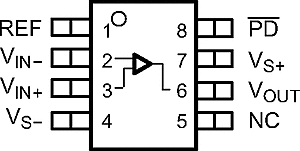
6 Pin Configuration and Functions
 Figure 6-1 DGN or DDA Package,
8-Pin SOIC, HVSSOP or SO-PowerPAD
THS3091 (Top View)
 Figure 6-2 DDA Package,
SO-PowerPAD
THS3095 (Top View)
Table 6-1 Pin Functions
| PIN | TYPE(1) | DESCRIPTION | ||
|---|---|---|---|---|
| NAME | NO. | |||
| THS3091 | THS3095 | |||
| NC | 1, 5, 8 | 5 | — | No connection |
| PD | — | 8 | I | Amplifier power down Low = amplifier disabled High (default) = amplifier enabled |
| REF | — | 1 | I | Voltage reference input to set PD threshold level |
| VIN– | 2 | 2 | I | Inverting input |
| VIN+ | 3 | 3 | I | Noninverting input |
| VOUT | 6 | 6 | O | Output of amplifier |
| VS– | 4 | 4 | P | Negative power supply |
| VS+ | 7 | 7 | P | Positive power supply |
(1) I= input, O = output, POW= power, and NC = no internal
connection